Version Notes
(Ver. 2.40.330 - January 7, 2021)
Summary
-
 Faulty gates support
 -
 Potentiometer-style Input Components
 -
 Multiplier Components
 -
 Pulse Width Modulator Component
 -
 Linear Gauge Components
 -
 XNOR gates now available
 -
 Custom Block Elements (CBE) pins
 -
 Component Guides
 -
 New "Bird's Eye View" window
 -
 New '.pbs' and '.cbe' file version
 -
 Component graphics changes
 -
 Maximum zoom factor increased
 -
 Clock Animation: Frequency and Enable Controls
 -
 Autoplay Mode
 -
 Bug Fixes
This version introduces the possibility of inserting faulty logic gates into the circuit (thanks to the suggestion of Arkadi Poliakov). Currently, only faulty gates NOT, AND, NAND, OR, NOR, XOR and XNOR can be inserted (bus type gates, and tri-state buffers are not available in the faulty version.
Instead of inserting a new component in the menu, the same component already available have been exploited. They have been re-designed to alter their behavior in simulation, blocking their output at a fixed (configurable) value.
To insert a faulty component, it is necessary to act on the menu item Faulty Component, available under the main menu Circuit (see the following figure). It opens a submenu, in which the two commands Set Mode ON and Fix Up All Faults are available.

The Set Mode ON menu command (or the shortcut <Control>+F) activates the faulty component mode.
The ![]() icon on the component bar, next to the logic gates, highlights that the mode have been entered (see the next figure).
icon on the component bar, next to the logic gates, highlights that the mode have been entered (see the next figure).

Only the logic gates remain available on the components bar.
All the other components are disabled, and also the simulation and the export on FPGA commands are disabled.
The faulty component mode is deactivated when a gate is inserted, or by clicking on the ![]() button (or pressing <Control>+F)).
button (or pressing <Control>+F)).
The faulty component will be inserted as the normal ones. However, immediately after the insertion, a small dialog will appear to set the desired Fault Type, as visible in the next figure.

After closing the dialog, the faulty component mode is automatically disabled. The faulty gates are graphically indistinguishable from the normal ones (once inserted, they appear as the others).
Note that if you rotate the component upon insertion, the faulty component mode is closed, so it is not currently possible to insert a rotated faulty gate. This inconvenience will be eliminated with the next version.
The Fix Up All Faults command (shown in the following figure) runs through the entire file and repairs all faulty logic gates (note that this command can not be undone).

Note that if a faulty component is copied and then pasted, the pasted component will be actually functional (the fault property is lost). Moreover, VHDL generation ignores the faulty property of the components, which are exported as working components.
New input components have been introduced, the 'Potentiometers', which generate 8 bit input easily and interactively. These components operate as a rotary potentiometer:

The two types have identical behavior, the only difference is in the position of the 'Zero'. The one on the left side generates numbers from 0 to 255, while the other one produces signed numbers, two's complement coded, in the range -128, +127. The new 'Potentiometer' Components are available under the Input Component menu, as shown in the next figure:

When inserting the component in the circuit, the Properties Dialog appears (see the figure below). In the dialog box it is possible to assign a label and to define the initial value generated by the component when starting the simulation "by animation". Note that the position 'zero' of the knob is marked with a dot (on its left most anti-clockwise position).
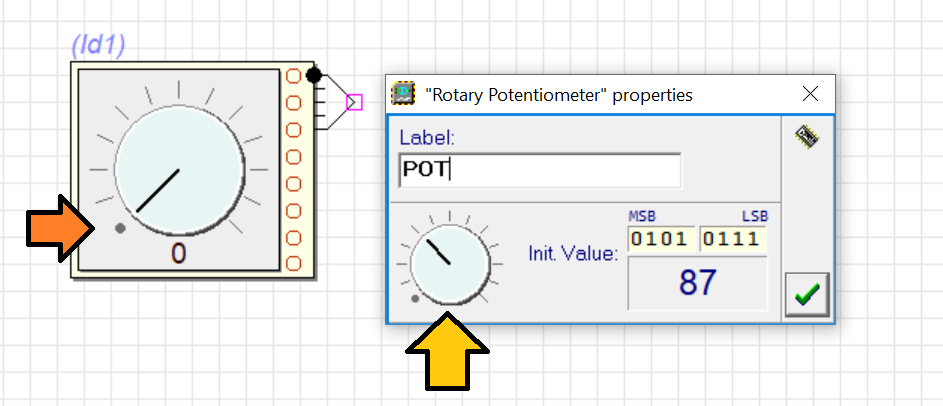
The angular position of the knob of the potentiometer is adjusted by clicking and dragging the mouse on the knob itself toward the desired position. Once the button of the mouse is pressed, it can be moved far from the knob in order to better adjust the desired angle. When the button of the mouse is released, the knob stably assumes the new position. The value is indicated in the dialog, in binary and in decimal. The reported figures refer to the type having the zero ('00000000') on the left side. The knob, when rotated completely clockwise, will give the value of 255 ('11111111'). The rotation range of the knob is approximately from 0 to 270 degrees.
The next figure shows, instead, the insertion of a zero-centered potentiometer type component. The knob, when fully rotated clockwise, will set the value to 127 ('01111111'). Turning it completely anti-clockwise, the value will be set to -128 ('10000000').

Example: in the following schematic, a potentiometer is exploited to adjust the frequency of a sine wave produced by a direct synthesis generator (click on the figure to open this example in the Deeds-DcS).
The generator reads the 8-bit samples of the sine wave from the 4Kx8 ROM memory. The samples are then displayed by an 8 bit DAC. The table in the ROM is addressed by the upper 12 bits of a 16 bit register, whose value is continuously increased, thanks to the adder, by a parameter set by the potentiometer. The generated frequency Fg is equal to Fg = Fck * K / 4096, where Fck is the clock frequency and K is the output value of the potentiometer component (0..255). Varying the angular position of the knob, it is possible to change interactively the frequency of the output sinewave.
In the timing diagram window, it is possible to define the value sequence of the potentiometer input track, as highlighted (in red) in the next screenshot:
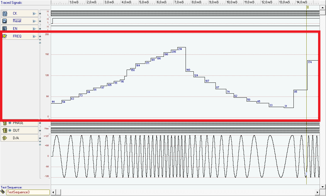
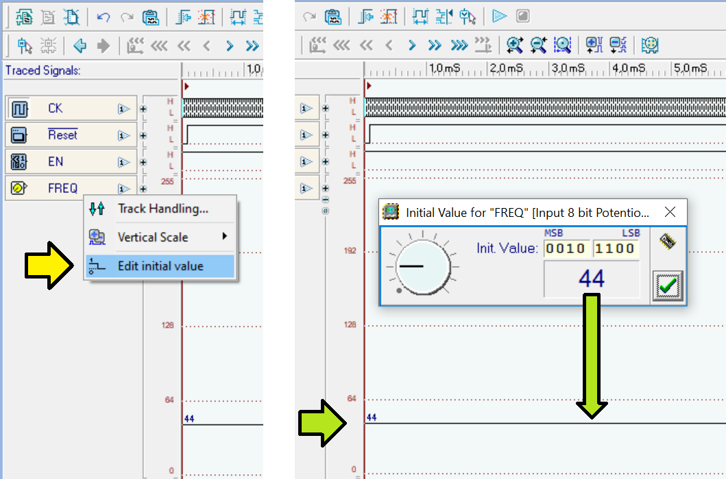
The sequence is defined manually, using the mouse, similarly to the other digital tracks. In this case, however, we define not only the transition time, but also the numerical value (in the range 0..255). In the next figure, the contest menu item and the dialog used to define the initial value are shown. In this example, the value is set to 44:
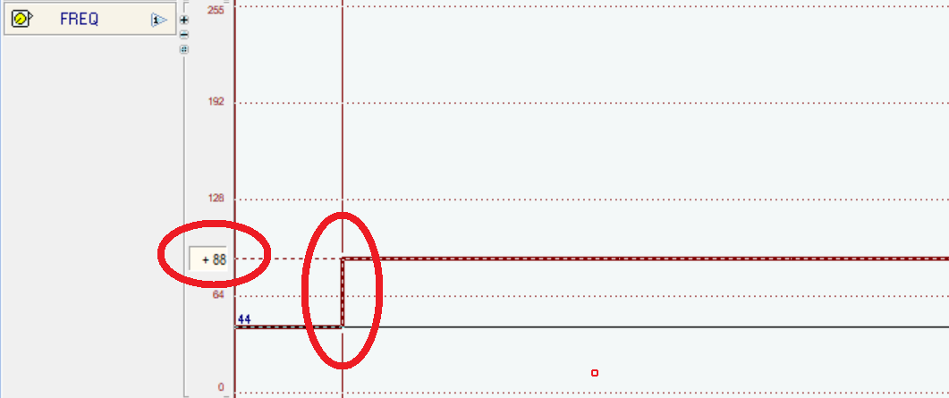
To insert new values for t > 0, you can click on the potentiometer track, and move the new vertex along the time and amplitude. With another click, the new value is set. On the left, you can see the value that you are entering:
Continuing the same operation, you can enter, step by step, all the desired values (note that, right now, it is not possible to enter ramps but only steps):
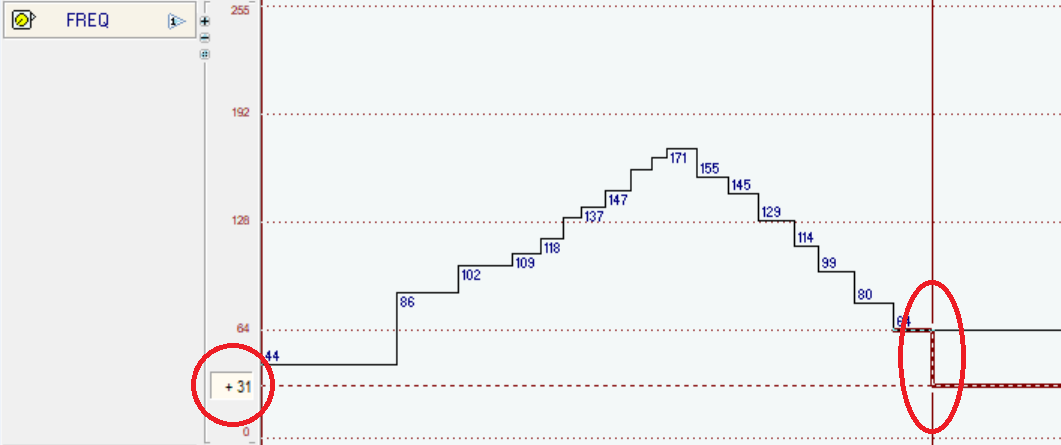
The values are visible near each variation (if the scale allows it). It is possible to add a new transition between two already existing ones, as shown in the example below:

You can also move edges and levels. In the next example, with the same command exploited before, we click on an existing edge of the waveform, catching it with the mouse. Moving the mouse (not dragging) we can change the time and level of the pre-existing transition. With another click, the changes are made persistent in the new position:

You can also delete edges. The delete command is activated with a click on the desired track, using the right button of the mouse. Then, we can click between two edges of the waveform, deleting the preceding transition, as shown in the next example:

Starting from this version, it is possible to implement prototypes on FPGA boards that use potentiometers as input devices. The following picture shows a potentiometer mounted on a small prototyping board, with the addition of a capacitor and some resistors. The four wires allow its connection to any FPGA board.

The user can "turn" a real knob, to provide to the FPGA card a parameter (coded with 8 bits). This can be done also with the little equipped cheapest cards (supported by Deeds). Normally, an Analog-to-Digital Converter (ADC) is needed to translate the potentiometer output voltage in a binary numeric value. Unfortunately, the majority of FPGA boards doesn't provide this tool, especially the cheapest ones.
Deeds tries to make up for this lack, embedding the functionality of the ADC inside the FPGA, at least for the digital part. However, it is still necessary to exploit a small analog external circuit which schematic is presented in the next figure.

Behind the scenes, Deeds implements a PWM (Pulse Width Modulation) signal generator, modulated by a ramp of 256 different values. We will get this signal on a pin of the FPGA (see the next figure, we call it 'PWM'). Another pin of the FPGA (which we call 'POT'), reads the algebraic sum of the PWM output and the voltage defined by the position of the potentiometer. The role of the capacitor is to filter the high frequency components of the PWM signal.. The other two wires must be connected to ground (GND) and to the supply voltage (+3.3V), normally available on the headers of most FPGA boards.
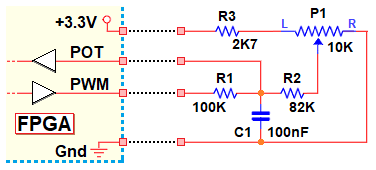
The embedded digital network is able to recognize, during the generation of the ramp, the crossing of the logical threshold of the POT input, thus saving the corresponding number. As the position of the potentiometer changes, the threshold will be crossed at different numbers. The values of the resistors are chosen so that we read the entire excursion of the 256 levels of the ramp (leaving a margin of excursion at the extremes of the rotation of the knob). The potentiometer is read about 8 times at second.
It should be noted that this is a relatively slow and qualitative system, but sufficient to read a knob controlled by a hand. If one wants the zero and the maximum number to correspond precisely to the limits of the excursion of the potentiometer, it is necessary to add some trimmers to adjust the resistors but, for educational purposes, we have seen that this is not strictly necessary.
How to associate the potentiometer to the FPGA pins
Let us choose a very simple network to test a prototype including a potentiometer on an Altera DE2 FPGA board. As shown in the next figure, a potentiometer is connected to a dual digit hex display, and to an 8 bit LED array (click on the figure to open this example in the Deeds-DcS):
Once the 'Test On FPGA' window has been opened, we can associate the potentiometer with the FPGA board connections. For this purpose, it is necessary to select the potentiometer on the circuit schematic appearing on the left side of the window (see next figure, arrow '1'). On the right side, a potentiometer connections panel will appear.

We have to associate the potentiometer circuit described before (shown in the window, see arrow '2') to the FPGA pins.
A list box (highlighted by arrow '3') allows you to select, one at a time, the required two POT or PWM connections.
A brief explanation, on the right side of the window (see arrow '4'), suggests the operations to be performed.
As shown in the figure, the POT line has been associated to the pin 'GPIO_1[01]' of the 'Header 0' connector (arrow '5').
The physical position of the pin is highlighted on the pin map (top view) of the connector.
The connector itself is shown on the FPGA board photo ('arrow 6').
After having assigned the PWM line to the pin 'GPIO_1[00]' of the same header, we continue assigning the other devices. The next figure shows the association of the dual hex display to a couple of seven segment display on the board.

The following figure reports the assignment of the 8 LEDs arrow component to the 8 green LEDs available on the board.

After the FPGA export process, we can see that the potentiometer circuit is built using two VHDL components. One component is the PWM ramp generator and, in all projects, it is always instantiated only once ('PotTimeBase' in the figure below). The other VHDL component will, on the other hand, be instantiated as many times as the number of potentiometers in the circuit, and contains the logic for reading the POT signal and for capturing the 8-bit number to be generated ('POT8').

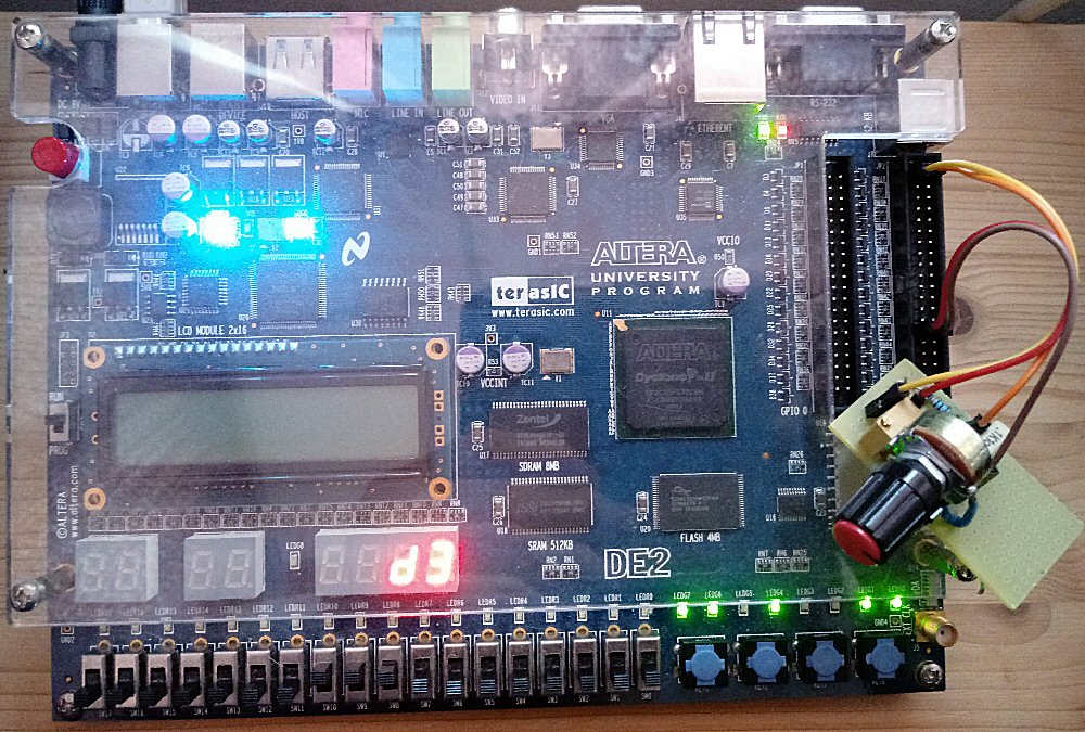
The following photo reports the potentiometer working on an Altera/Terasic DE2 board adjusted to generate the number D3h on the display of the board, and the corresponding '11010011' on the 8 green LEDs on the bottom right.
Starting from this version, a new group of arithmetic components is available in Deeds, the Multipliers. They have been tested not only in the simulation environment but also on FPGA boards (thanks to Edoardo Ragusa for the help he gave me regarding their VHDL encoding). The next figure shows the menu items that allow to insert the multipliers in the schematic:
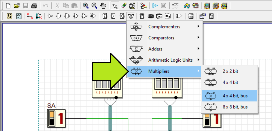
Four different components are available (see the next figure):

The simplest one is a 2x2 bit type (the leftmost in the figure), that works with unsigned numbers. The second and the third one are 4x4 bit types, useful for both signed and unsigned numbers. They are identical, except for the pins (normal or bus type). The last one allows multiplication of two 8-bit numbers (signed or unsigned), producing a 16 bit result. The signed numbers must be two's complement coded.
Apart from the first one, all the others have a programming pin for each of the two operands. The pin sA allows you to specify whether the operand A is signed (sA = 1) or unsigned (sA = 0). Same functionality for pin sB, that refers to the operand B (note that the result is signed if at least one of the two operands is signed).
The figure below shows a simple test circuit for the 4x4 bit type (click on the figure to open it in the Deeds-DcS).
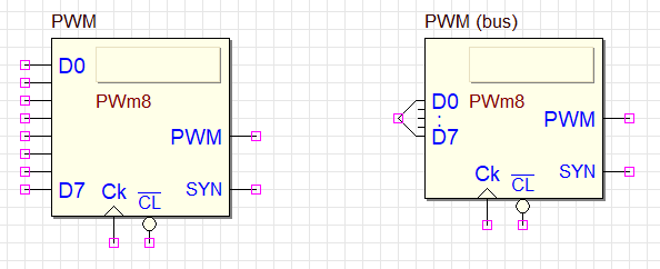
The new Pulse Width Modulator component (PWM) has been added to the library. The size of the input data is 8 bits, and two versions are available, with normal or bus inputs (see the next figure).
The PWM components are available in the counters group, as shown in the next figure.

The PWM output has a period equal to the frequency of the clock Ck, divided by 256. The duration of the high part of the PWM signal equals the number presented at the data inputs D7..D0. If the number is 255 ('11111111'), the duration will be 255/256 of the period. If the number is one ('00000001'), it will be 1/256. If the number is zero, the output is constantly low.
The PWM output goes high on the clock edge following the cycle in which the number on the counter equals the number at the input D7..D0. The PWM output goes low on the clock edge following the cycle where the number on the counter reaches zero.
The SYN synchronization output is activated every 256 clock cycles and corresponds to the end of the pulse generation, i.e. the end of the down count of the internal counter, which counts from 255 to 0. The number D7..D0 is acquired on the clock rising edge at the end of SYN pulse, so the PWM output will assume the new duty-cycle without spurious transients.
The user can assign a label to the symbol. During the simulation 'By Animation', the PWM symbol is animated and shows a sort of progress bar which represents a cycle of the PWM output, with duty-cycle proportional to the number set on D7..D0. Thew following figure shows an example of usage of the PWM component (click on the figure to open it in the Deeds-DcS).
An example of Timing Diagram simulation of the PWM component is visible in the next figure. The PWM modulator track (see the highlight) shows the value that it acquires from the input D7..D0.

The PWM output track shows a series of pulses of different duration (0/256, 58/256, 224/256, 3/256...) according to the values set to the input (by means of the potentiometer component).
With this release, output devices specifically designed for animation purpose, called Linear Gauge components, are now available. A Linear Gauge displays an output in 'analog' mode, similar to a column of LEDs (or the classic 'progress bar'). See the examples below (click on the figure to open it in the Deeds-DcS).
They look like a ruler with notches. In order not to complicate the representation, only the zero value is reported on the scale. The actual value is represented in numerical form. Linear Gauges are available in the output components group and are available in the 4 and 8 bit versions, as shown in the next figure.

The properties dialog box allows you to define whether the zero is to be placed on the left side or centered.

In the timing diagram the Linear Gauges are very similar to the digital-to-analog converters (DACs) and represent the output in 'psuedo-analog' mode.

Linear Gauges are intended for simulation only and do not generate VHDL code (they are not exported).
Starting from the current release, XNOR gates (negated XOR) are introduced in the component bar (see the screenshot below):

The new components are available in the 2, 3, 4, 5, 6 and 8 inputs version, as shown in the following picture:

The PIN components of the Circuit Block Elements (CBE) have been updated, increasing the choice in the available sizes, now from two by two up to 24 wires (4, 6, 8, 10, 12, 14, 16, 18, 20, 22 , 24) and a 32-bit PIN are available (see a few examples below).

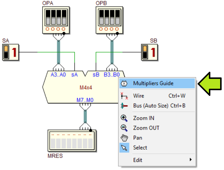
Now a few guides are available in the main menu, regarding the recently introduced components (see the figure below).

The same guides are available in the Context Menu of the components, as shown in the next example, about a multiplier:
A new navigation window for the circuit diagram, called Bird's Eye View, has been now introduced. It can be activated using the menu item under 'View' (see figure below), or using the shortcut "F3".

The Bird's Eye View window opens, by default, on the bottom left of the editor (see the figure below). Then, you can move it when and where you want, in a position that is reflected in the main window (moving this will also move the Bird's Eye View window).

The window can be closed with the same short cut (F3). When it is reopened, it will appear in the last visualized relative position. If multiple instances of the Deeds-DcS are contemporary opened, only the Bird's Eye View window of the currently active instance is visible. The content of the window is then updated following any modification of the schematic in the circuit editor. The size of the Bird's Eye View window is set automatically, it cannot be changed, and depends on the size of the circuit drawing.
A rectangular red frame is visible in the Bird's Eye (see the previous figure), showing the circuit area currently visible in the editor in the main window. By moving or zooming the view of the circuit in the editor the position and size of the red frame is updated. By clicking in the Bird's Eye View window, the current view of the editor will be automatically moved to the new position. Moreover, by turning the mouse wheel on the Bird's Eye View, it is possible to control the zoom factor of the circuit.
The internal file format of the '.pbs' and '.cbe' files has changed (version '1.036'). The change has been required because of the addition of new components and new features. The old files are readable by the new Deeds version, while files created by the current version are not compatible with the older Deeds-DcS releases.
The size of the component representing the 'low' constant ('0') has been reduced, so that they can now be placed side by side a little bit closer, matching its size with the one indicating the 'high' constant ('1'). Now they appear as follows (shown in the next figure).

The maximum zoom factor of the diagram in the circuit editor of Deeds-DcS has been increased from 9 to 12, to facilitate the vision of the circuits even with high resolution (4K) monitors. Consequently, the maximum zoom factor is increased to 12 also in the "Save Circuit Image" dialog, in the case of "Web Quality" images (96 pixels / inch), see the following figure:

From this version there is a new management of the clock animation speed control and clock animation enabling. Previously, these settings were global and persistent (saved in the Registry).
From the current version, however, these two parameters are saved in the circuit file, in order to memorize the animation speed and the enabling of the clock in a convenient and consistent way with the type of circuit to be simulated. The simulation command bar has been moved to the bottom of the window, to make the control parameters more easily available (see the next figure).

When creating a new file, or opening a file created with a previous version of Deeds, the speed of the clock animation is set by default to 2Hz and its animation is NOT enabled (after, the two settings can be freely changed). Changing the two parameters forces you to save the file if you want to keep the new setting. If the simulation (by animation) is in progress, however, we can freely modify both the animation speed of the clocks and its enabling, without modifying the file.
If, during simulation, you want to keep the new setting stored in the file, you must use the Save as Default button, which appears only during simulation, remaining disabled until you'll change the parameters. Otherwise, when returning to the editor, the previously saved values will be restored (the button is shown in the figure below).

Note that these commands cannot be undone.
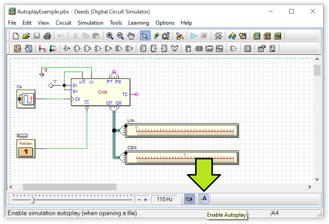
The possibility of activating the simulation by animation automatically when opening the circuit file (only for .pbs files) has been introduced. The Enable Autoplay button is now present in the simulation command bar and it is visible when the simulation is not active. See the example below (click on the figure to open it in the Deeds-DcS).
If one clicks on the Enable Autoplay button, the following message warns that the Autoplay function will be activated:
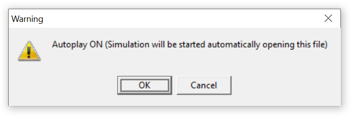
If you answer OK, the mode will be active, and the bar changes its appearance, showing two other buttons (Hide Menu and Test Autoplay mode), see the figure below.


By clicking on the button Hide Menu, a message will warn you that the menus and command bars will be hidden from the user while Autoplay is running.
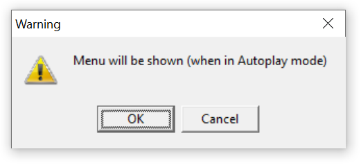
By acting on the same button again, it is possible to disable this mode and the menus and command bars will be visible during the autoplay mode. By clicking on the Test Autoplay Mode button, instead, we can test these settings, simulating the Autoplay mode (in this case you are forced to save the file).
By saving the file, the autoplay mode will be available. The next time the file will be opened, it will automatically enter the simulation (by animation) with, or without, menus and command bars, as set. If you click on the schematic below, the circuit will be opened in the Deeds-DcS, in autoplay mode.
By pressing the Exit Autoplay button on the simulation bar, or the
Multiplexer Animation
Fixed a bug regarding the Multiplexers.
If the simulation was started with one or more selection inputs in the Unknown state, the highlighting of the selection (see an example in the following figure), showed channel zero selected, rather than none.

Signal value display during the Simulation 'By Animation'
The Clock and other single output components, like the LED, and the One Bit Output, beyond a certain number of variations per second, show a value that is not the real one, but one flashing at a frequency of about 12.5 Hz, to avoid visual stroboscopic effects.
Due to a bug, when the real variation of the output stopped, the display remained on a random value, and not on the one defined by the simulation. Now the problem has been solved.
DMC8 Memory Windows during the simulation by animation
In simulation by animation, sometimes there was a serious slowdown in execution, caused by incorrect management of the debugger windows update, in particular regarding the memory display window.
The issue was addressed by slowing down the updating rate of the debugger windows (now every 20 mS).
Saving the circuit file during the Simulation 'By Animation'
Saving the file during the simulation produced a halt to the simulation which could cause crashes when restarting it.
Now the problem has been fixed, stopping the simulation correctly before saving the file.
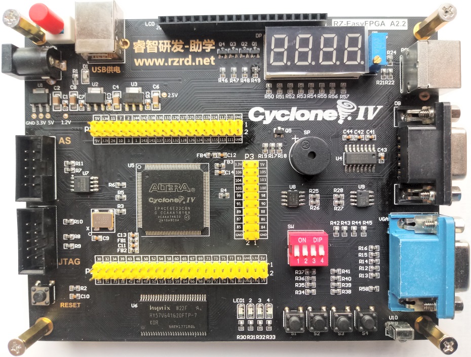
Support for the RZ-EasyFPGA board has been added. This card (see: www.rzrd.net) is quite inexpensive and easy to find online (see the next picture).
In the next figure we see a simple three-bit counter, with enable (click on the figure to open this example in the Deeds-DcS).
By opening the Test On FPGA window, it is now possible to select the new board among those available, and then to associate all the schematic input and output components to the available physically ones on board, as usual (see the next figure).

The next figure, which shows the Assignment Summary window, lists the resulting associations. Observe that the clock has been set at a very low frequency (5Hz), so that we can observe the counting sequence. Now we are ready to test our counter on the new board.

Keep in mind, when using this card, that the push-buttons, switches, LEDs and all the other devices on board are connected also to the connectors (P1, P2 and P3). This can be a disadvantage, as the manufacturer does not make freely usable FPGA pins available, and you should pay close attention to the schematic of the board (available here) to verify the pins that can actually be used for your project.
In any case, the advantage is that the present components are all usable by Deeds, even if with the due care mentioned above, as each of their connections can be assigned through a connection to the connectors pins. Moreover, Deeds also shows the names of the pins of the available components in the pin lists of the connectors, with the add of the device pin names (assigned by the manufacturer), as shown in the next example:

Deeds manages the cross compatibility between the use of push-buttons and switches of this board, which the manufacturer has unfortunately connected to the same pins of the FPGA. Therefore, if in the 'Test On FPGA' window we associate a switch to an input component, Deeds will automatically prevent from using that push-button (that share the same pin), and vice-versa.
In the next figure (left hand side), the switch 'Sw1' is assigned to one component of the schematic. Then, when trying to assign the push-button 'S1' resource to another component, it will result 'not available' (right hand side), because Sw1 and S1 share the same FPGA pin (88).

The four digit seven-segment display available on the board cannot be immediately associated with the displays available in Deeds. Indeed, the four digits are managed in multiplex mode (see the next schematic, from the referenced documentation), and right now it is not directly supported by Deeds.
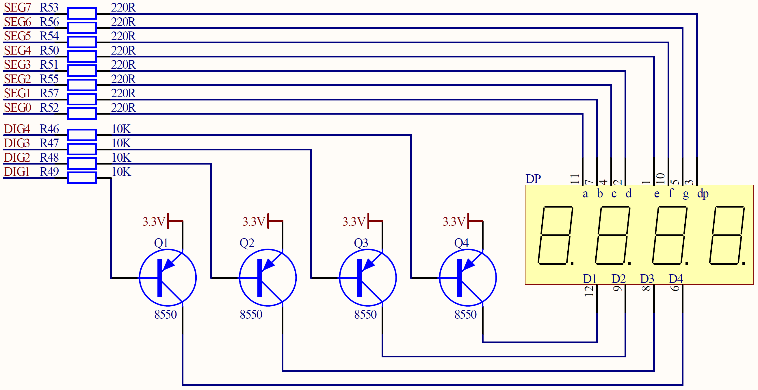
In any case, it can be always used by means of the relative pins available on the connectors (see the next figure).

In the 'Test On FPGA Window' we added the possibility to use the central mouse wheel to zoom both the circuit schematic and the photo of the FPGA board in use.
Fixed a BUG concerning the export of the DMC8 Enhanced Microcomputer component to VHDL. Under particular conditions, the addresses of the ports IE..IH and OE..OH were exported with their default value (04..07, respectively) even if their value was defined differently.
Now, the pseudo-analog traces, such as those of digital-to-analog converters (DACs), linear gauges, and potentiometers, show their value alongside each variation. If the horizontal space for drawing the number is insufficient, depending on the scale of representation, the number is not drawn. Also, when creating this type of track for the first time, the vertical zoom is set by default higher than the others.

The possibility of directly editing the input tracks represented in hexadecimal (HEX) has been added. Previously, these tracks were only editable by expanding them into binary tracks, and editing the individual tracks individually (see the following figure).
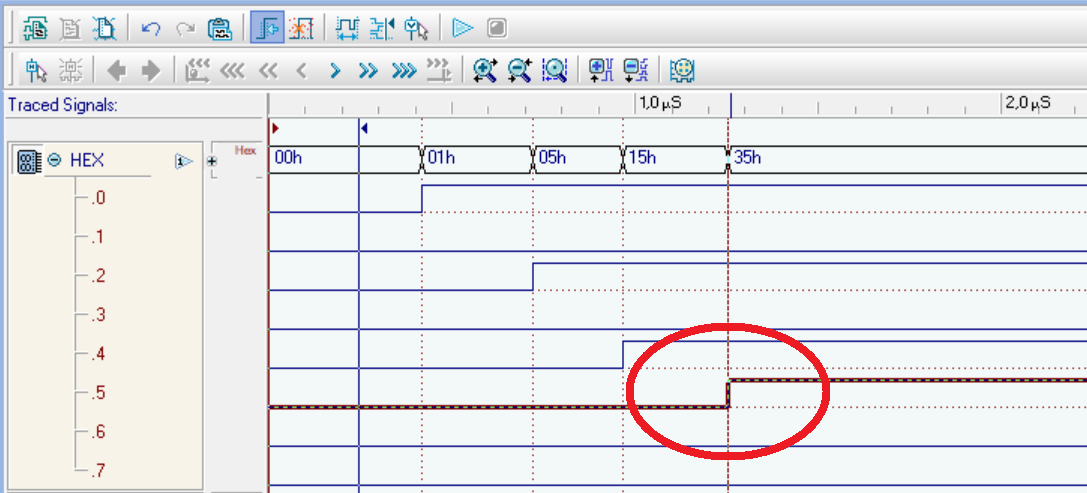
Now you can edit the HEX track too. To add a new HEX value, click on the track to enter the editing mode (visible in the next picture).
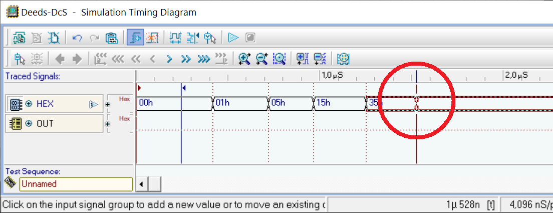
Using the mouse, move the proposed transition on the desired time. Another click will open a small dialog box, as shown below, displaying the current value corresponding to the selected time.

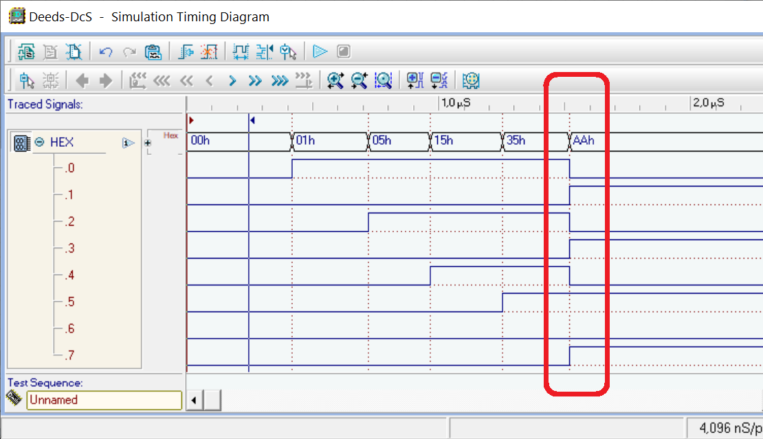
Enter a new value and press OK. The track will appear as visible in the next figure. In this example, the new entered value is AAh.

By opening the subtracks, the result will be as shown in the next figure. Of course, it is also possible to edit the single binary tracks in the usual way.
In a way similar to the one used for the binary track, it is possible to move or delete an existing HEX value. A mouse right click on a track is the short cut to enter (or exit) the delete mode.
Timing diagram redrawing
When redrawing the contents of the timing diagram window (for example after a simulation step), the windows of all open applications were updated too, resulting in an annoying screen flicker.
This problem has now been solved.
Closing application during timing simulation
If a long-processing simulation was running in the Timing Diagram, when attempting to close the application main window, a crash was generated, reporting an 'out of bound' error.
The problem has now been solved.
Saving file during timing simulation
If the timing diagram was started without saving the file, a 'Save As' can be performed anyway.
This operation, depending on the case, could result in a crash in the simulation.
Now, if the simulation is not in progress, the user is warned that the timing diagram will be closed before.
Otherwise, if the simulation is running, the user is warned to pause the simulation, before saving the file.
Font Size Change
The command to change the font size caused the caret to be moved at the beginning of the file.
Now the problem has been solved, and the caret stays where it should.
Right bracket character
Sometimes, the right bracket key on the keyboard inserted the character at the beginning of the file, while enlarging the font size in the editor by one.
This bug has now been fixed.
Now a double click on an object opens the properties window in relation to the object itself (thanks to Francisco Gonzalez for the suggestion).
