Deeds Screenshots

The following screenshots provide a hint on how Deeds tools can be used for a project, using different techniques of digital design, stand alone or combined together.
(For more info, read the Demos Pages and the Version Notes ).
Learning Materials |
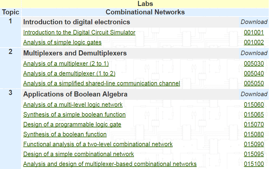
In the next figure, see a little part of the Learning Materials main index, available on this web site:
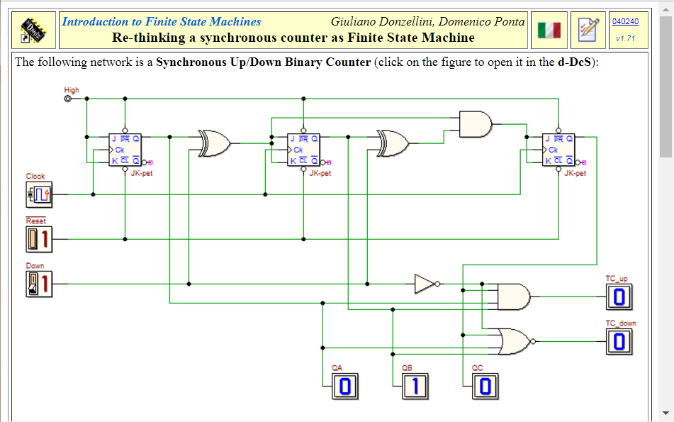
When the student clicks on a title, the corresponding Deeds laboratory page is opened, showing the assignment (see the following figure). In this example, the assignment asks the user to verify the behavior of the circuit shown in the figure, using the Deeds-DcS (Digital Circuit Simulator):
All objects that the web page visualizes can be made “active”: in this example, by clicking on the figure showing the schematics, the Deeds-DcS will be started, opening the circuit, ready to be analyzed and simulated.
Deeds-DcS (Digital Circuit Simulator) |
The Deeds-DcS allows all the basic operations that professional simulator do, with a special orientation to the educational needs. For instance, the components available on the bin have been defined to be simple to understand. We avoided on purpose the use of complex real component, that could confuse the beginner.
Also, input connections are implemented as Logic Switches, Push-Buttons; even the Clock Components are seen as inputs. Outputs are shown as LEDs or Displays components.
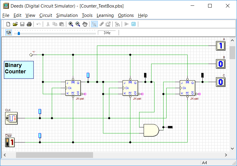
The Input Components can be clicked to stimulate the circuit, producing an animation of it. The following figure shows an example of the Input / Output components used to interact with the network:
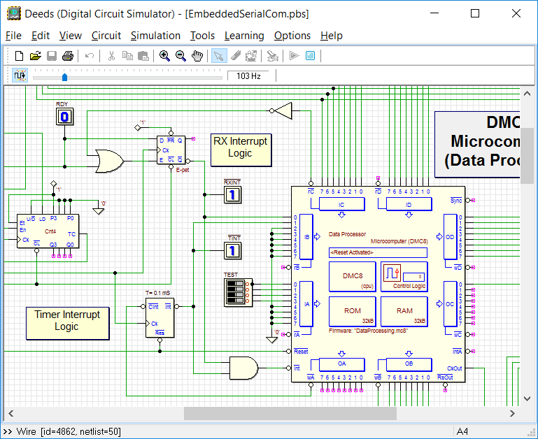
Below, an example of a circuit based on a microcomputer component is shown:
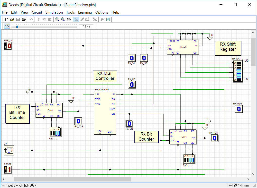
The next one shows a digital system including spare logic as well shift registers, counters and a custom component ("RX MSF Controller", in the schematic), designed with the Deeds-FsM (Finite State Machine Simulator) (see later):
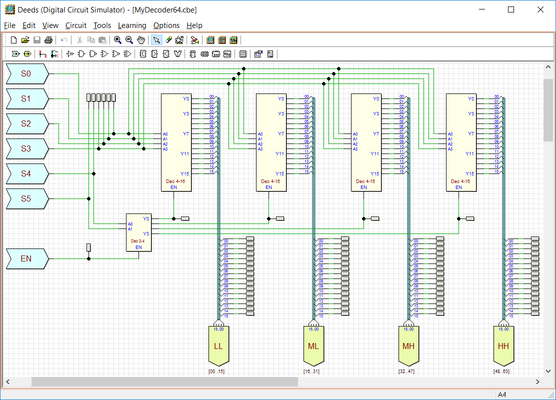
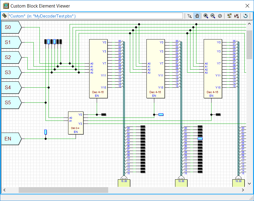
The Deeds-DcS allows to build components that can be reused. The Circuit Block Elements (CBE) components are user-defined in terms of schematics, enclosed within a component symbol. In the next figure, the schematic of a decoder 6 to 64 lines, enclosed within a CBE , is opened in the Deeds-DcS:
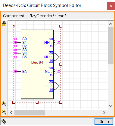
The user defines the aspect of a new CBE component through the Symbol Editor (see the next figure), integrated into the Deeds-DcS. After saving the “.cbe” file, it becomes available to be inserted into an ordinary schematic (".pbs"):
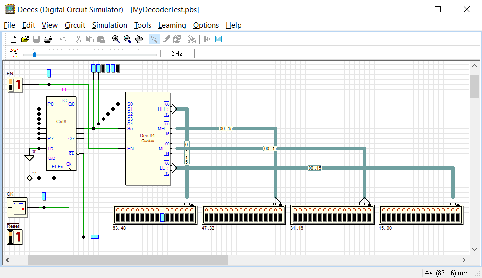
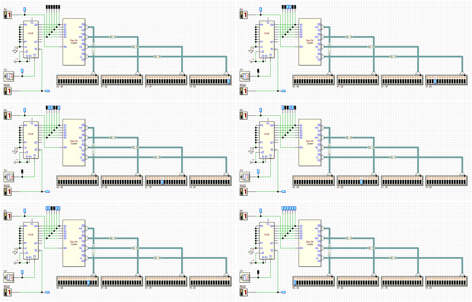
In the following figure, the example shows the same CBE, connected as a normal library component: a binary counter drives the decoder inputs, and its outputs are connected to 64 LEDs:
During the Simulation by Animation, you can observe also the activity of the CBE internals, simply with a click on the CBE component: the CBE Viewer will show the animation of the internal schematic.
An example of Simulation by Animation of the "main" circuit is given by the following GIF:
Note that, currently, a CBE can not contain other CBE components; however, it may contain any other component, such as Finite State Machines and/or a Microcomputer.
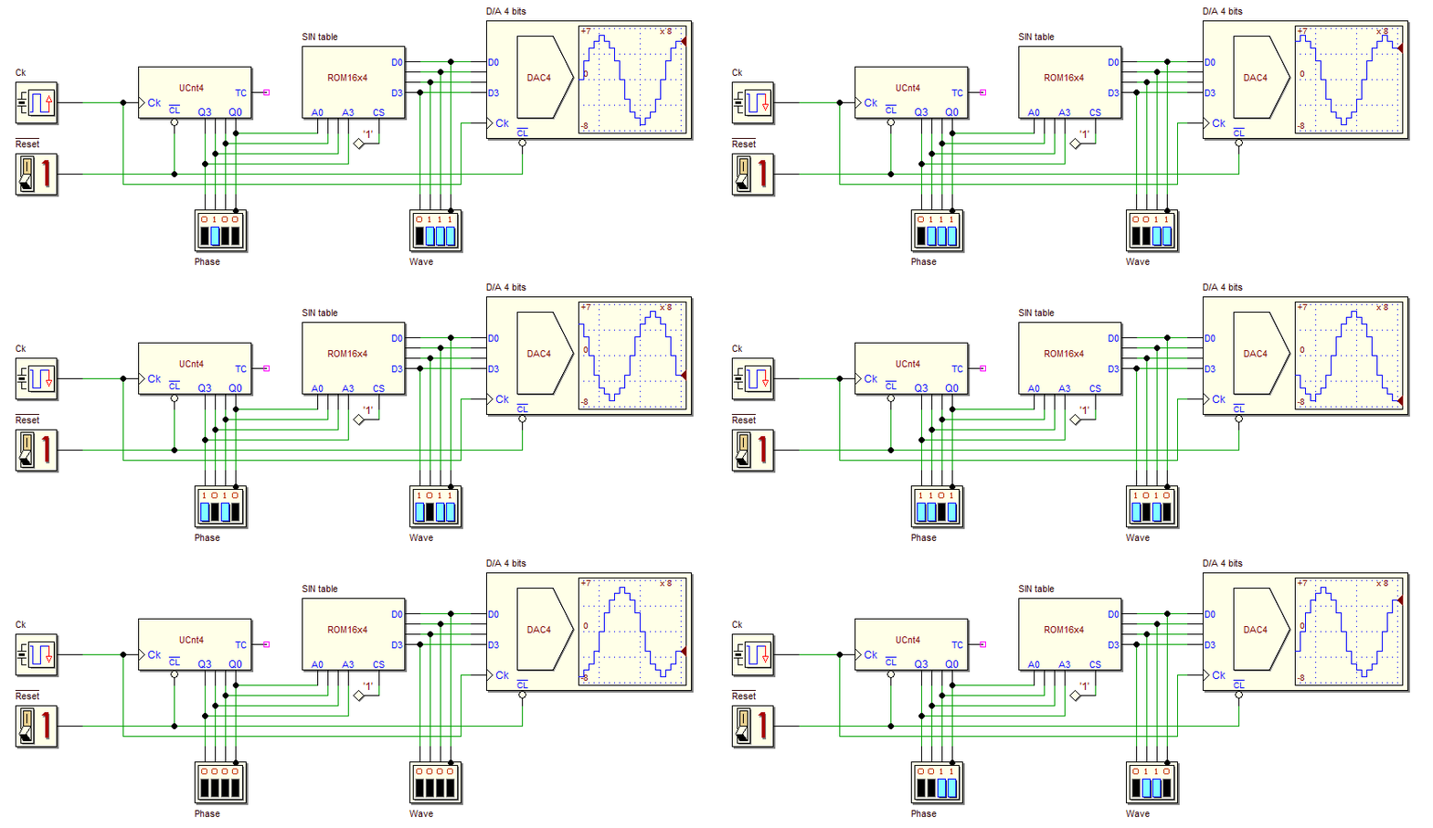
ROM and RAM memory are available in the Deeds-DcS tool. Digital to Analog Converter (DAC) component are available too. The following animated GIF presents a little example of this kind of components, used to generate a sine wave digital signal. In this network, a 4-bits counter addresses a ROM 16x4, containing the sine wave samples; then, the DAC converts each sample in a "analogic-like" value, shown in the DAC itself:
To get some other informations about the DAC usage, please go to the DAC examples, in the demos pages.
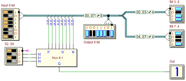
Bus Connections can be used to join components. As in the figure below, a Bus is equivalent to a group of wires, and is represented as a colored thick line:

The number of wires that a Bus groups together is the Bus Size. We introduced also a new type of pin (the Bus Pin), designed to connect a component directly to a Bus: we use Bus Pins to make the schematics more readable and concise. In the next figure, you see some example of Bus, Tap, Splitter and Wire Connections:
In the animated figure that follows, we present an 8-bits Adder component at work, Bus connected, for different input values:

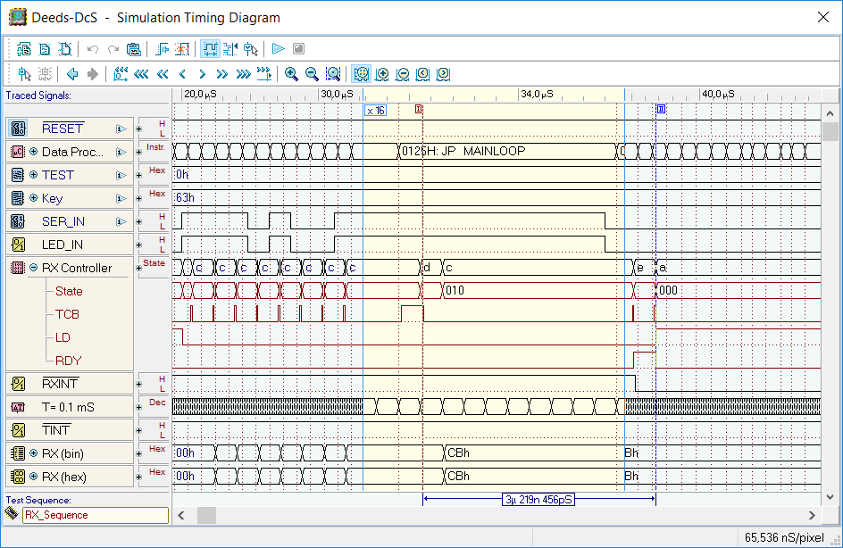
The Deeds-DcS, as the professional simulators do, allows Timing Simulation of the logic networks. To help the beginner, timing simulation can be obtained interactively, with a step-by-step approach, or can be run in a defined time interval. As in the professional tools. Simulation takes into account the time delay of components, to produce a near-real-case simulation. Input sequences (input test vectors) can be saved and re-loaded in the diagram. Cursors are available for time measurements, as shown in the following screenshot:
When simulating a system that includes a microcomputer, the timing diagram can show the microprocessor state and trace the instruction execution:
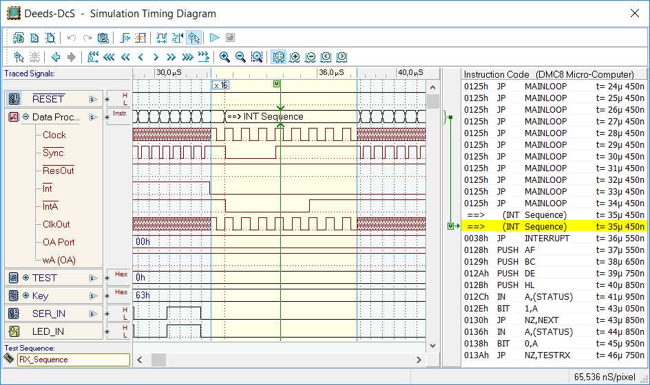
The Deeds-DcS, starting from Ver. 1.5, has been enhanced with the capability to export your entire project in VHDL language and test it on FPGA boards:
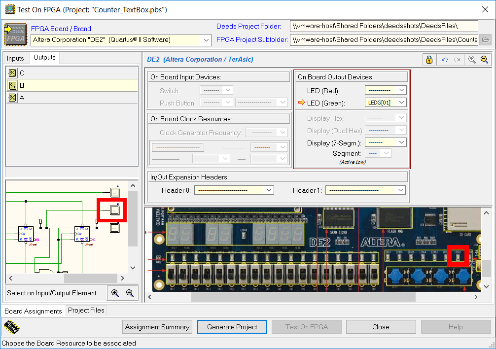
In the figure above, you see a view of the "Test on FPGA" expert window, included in the Deeds-DcS, that allows to configure the associations between the schematics and the FPGA board resources (see later in this page).
Deeds-FsM (Finite State Machine Simulator) |
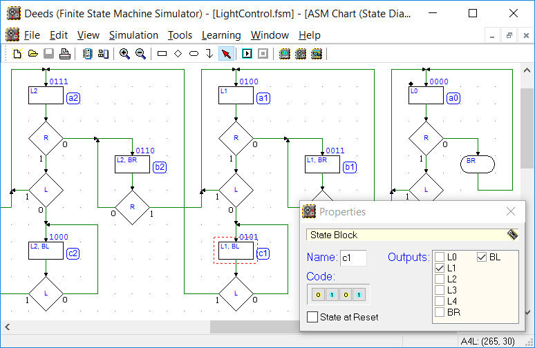
This tool allows the design of custom components modeled as Finite State Machines (FSM). These can be designed using the Algorithmic State Machine charts (ASM). In the screenshot below, an FSM component under design is shown. In this example, the properties window, displayed on the right, allows to set all the required parameters for each object included in the chart:
The FSM component can be functionally simulated directly in the Deeds-FsM, before inserting it in a Deeds-DcS schematic. The user can check the functionality of the component, state by state, as shown in the next screenshot:
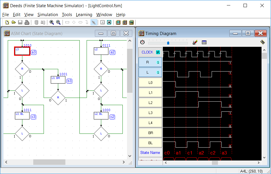
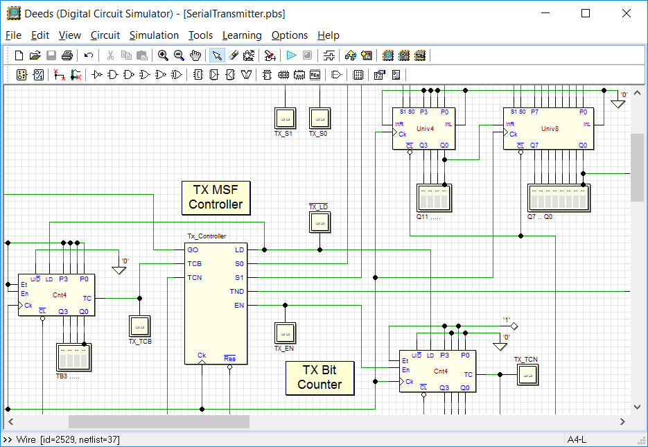
Then, the new custom FSM component can be inserted in the Deeds-DcS. The user connects as usual the custom component to the other components in the schematic, and then simulates the system. In the next example, a FSM component has been inserted, as system controller (see the TX Controller component), into the schematic of a serial transmitter:
Deeds-McE (Micro Computer Emulator) |
The microcomputer emulated by the Deeds-McE is built around an 8-bit microprocessor, RAM and ROM memory and a simplified parallel I/O port system, whose address can be user defined. User can also define the ROM and RAM memory size.
The tool includes an assembly code editor with undo/redo capability and text syntax highlighting, a two-pass assembler and an interactive register-level visual debugger.
The "DMC8 Basic" microcomputer architecture is shown in the following picture:
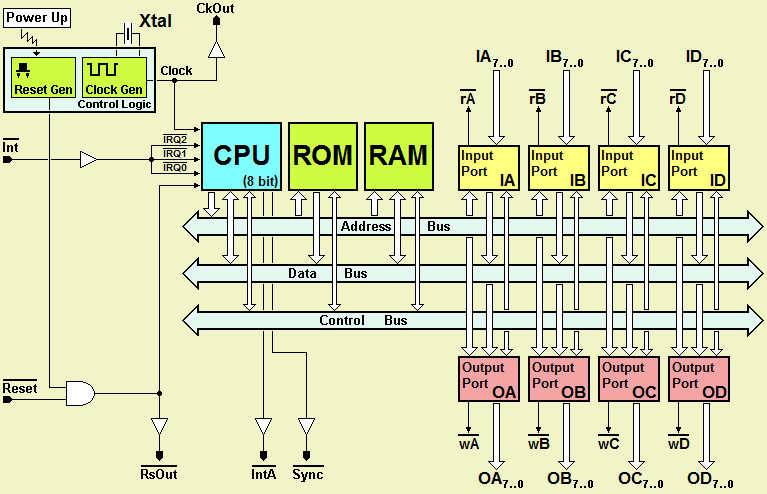
In the next figure, the "DMC8 Enhanced" version of the microcomputer:
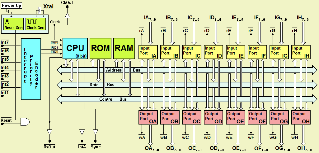
The microcomputers are programmble using assembly language, and you can choose between DMC8 instruction set (Z80-like) and D8080 instruction set (i8080-like). All the documentation regarding the microcomputer systems is available here.
The microcomputer can be inserted in the schematic editor of the Deeds-DcS (as seen before), allowing the simulation of digital systems with embedded processor.
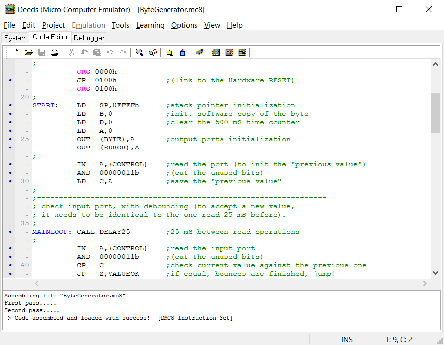
The next figure shows the Assembly Code Editor. Syntax highlighting helps the user in understanding the code. Assembling and linking are transparent to the user: after the compile operations, the machine object code is automatically loaded into the emulated memory (as if we had a ROM programmer):
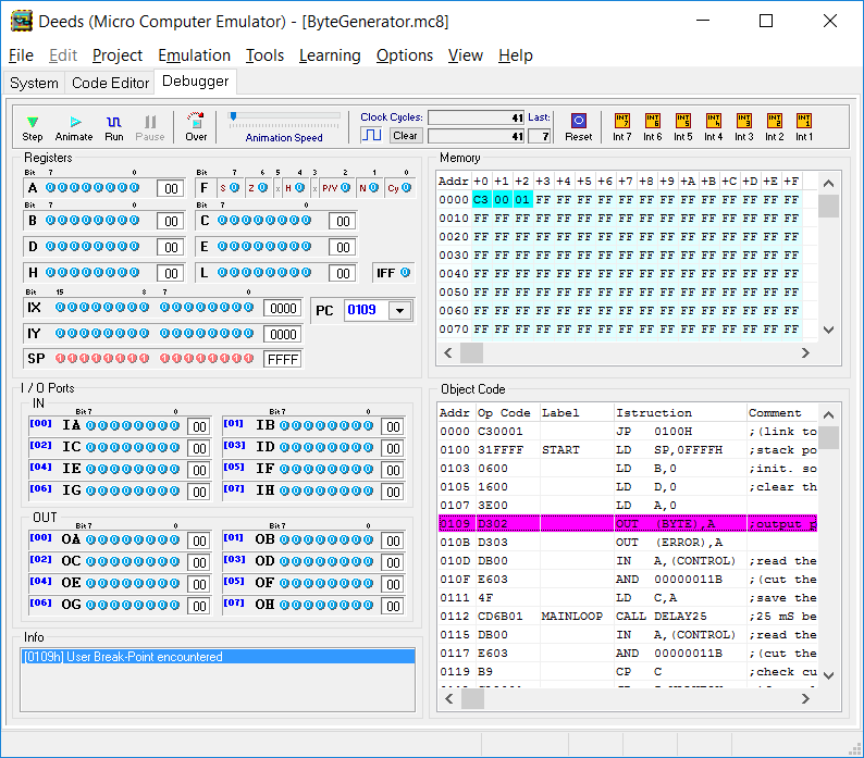
The Assembly Code Debugger allows a full control of the microcomputer operations, including parallel I/O operations and interrupts. An animation mode permits to execute the code under the control of the student, that can dynamically modify I/O values and simulate interrupts.
FPGA Support |
Deeds introduces students to the use of Field Programmable Gate Arrays (FPGA) in digital design, in a very simple way. Deeds makes the process of FPGA configuration straightforward and compatible with the beginners’ skills, integrating FPGA configuration and testing into its interactive design and simulation flow. Combinational and sequential circuit design, as well as microprocessor programming and interfacing, became demonstrable through physical FPGA boards, in a way fully compatible with the beginner's skills.
Deeds allows the compilation of a project into an FPGA chip starting from the Deeds-DcS, leaving in the background the operations performed by the FPGA-specific EDA tool (that is anyway necessary). Beginner users need no knowledge of Hardware Description Languages (HDL) and they can not interact with the FPGA-specific EDA tool except for the FPGA project compilation.
The student can test its digital system on a commercial-available FPGA board. The project can contain all combinational and sequential components, any number of Finite State Machines, and the DMC8 microcomputer component. In the Deeds-DcS, two commands are available: "Export VHDL" and "Test on FPGA" (see the next figure):
The command "Export VHDL" opens a dialog window and, at the same time, starts the VHDL conversion of the file currently opened in the schematic editor. At the end of the conversion, the user will find one or more VHDL files opened in the multi-folder dialog window, as you see in the next figure:
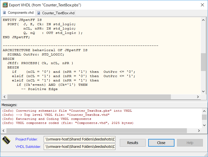
All the VHDL files are automatically saved in a subdirectory (for instance, if the original file is named "Counter.pbs" and it is located in the directory "D:\Circuits\", the new subdirectory will be "D:\Circuits\Counter_VHDL\"). Note that this command is useful to reuse the VHDL code in another project, but it doesn’t prepare directly files for FPGA implementation, as the other command does. All the library components and the Finite State Machines are exported in behavioral VHDL, while the top level schematic is compiled in structural VHDL.
The command "Test on FPGA" opens an expert window that allows to choose a FPGA board and to associate all the Input/Output components of your schematic to the FPGA board devices and resources (see next next figure):
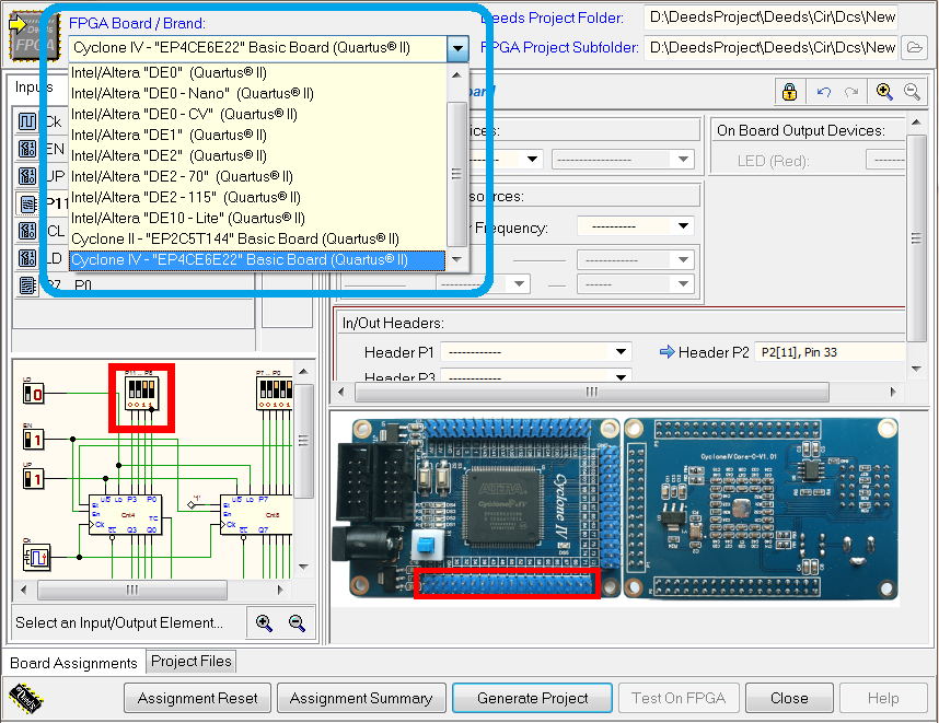
A few FPGA boards by Terasic, based on an Altera Corporation FPGA, are supported:
DE0, DE0-Nano, DE0-CV, DE1, DE2, DE2-70, DE2-115, DE10-Lite.
Moreover, support has been added for two small and inexpensive FPGA boards, based on the Cyclone II "EP2C5T144C8N" and Altera Cyclone IV "EP4CE6E22C8N" chips:

After the choice of the FPGA board (here the "DE2" model), the user implements the associations by selecting (on the left hand side) each Input or Output termination and (on the right hand side) selecting a corresponding device available on the board. The highlighting of the selected objects in the schematic and in the board image will help in this process. In the following figure is put in evidence the associations needed for a Clock Input component, that needs to be set, defining a suitable frequency for the test of the system (in this example, 50Hz):
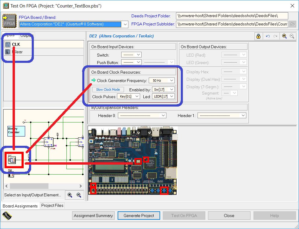
The component that can be "associated" are: switches, push buttons, clock resources, leds, hex displays, and connectors. Note that the on board clocks can be internally "scaled" to various frequencies, so that the user can choose the preferred one. Moreover, a Slow Clock Mode allows to set, on the board (at run time), the clock mode: for instance generating a very slow frequency value or advancing the clock "cycle by cycle" using one of the push-buttons available on the board.
Tutorials are available, to provide a synthetic introduction to FPGA projects, in the Learning Materials page.
