Version Notes
(Ver. 2.20.190 - Dec 29, 2018)
 Deeds-DcS (Editor)
 Tri-state and Bidirectional Buffers
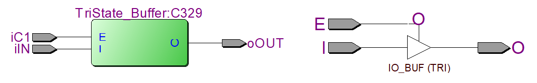
Tri-state and Bidirectional Buffers have been added to the component library. The following figure shows an example of usage of the Tri-state buffers:

In this example IN1, IN2, IN3 and IN4 are four data inputs. C1, C2, C3 and C4 are the corresponding 'Enable' lines that control the activity of each tri-state buffer (only one Enable must be set at a time). The figure shows the circuit during a 'Simulation by Animation' session, where the only active buffer is the one driven by the C2 line, that is set. The simulator highlights the active buffer with a different color. All the other ones are in 'high-impedance' ('Hi-Z') (i.e., electrically disconnected from the output line OUT). The result is that OUT = IN2.
The logical behavior of this network is similar to that of a Multiplexer '4 to 1', with the difference that using the tri-state technique we use less wire connections. The following example compares the tri-state connection of four modules (where we use only one line to bring data) against a multiplexer-style connection (that uses four lines instead):

Increasing the number of connected modules, we should substitute the multiplexer with a bigger type, adding a wire for each added module. Using the tri-state style connection, instead, the wire will remain only one (we don't discuss here the selection logic).
The Tri-state Components are available under the 'Buffers' icon, on the Component Tool Bar, as shown in the following figure:
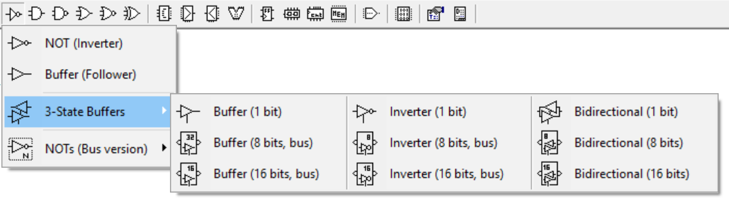
Three buffer types are available. In the following figure, the non-inverting buffers, in 'one bit' and in '8 or 16 bit bus' version:

Here the inverting buffers (same sizes):

Finally, the bidirectional buffers (non-inverting):

Note: starting from the current version, all wires and busses are usable in a bidirectional way. In the figure below, an example of bidirectional connection (1 bit):

In this basic example, caught during simulation, the color highlighting the components shows that input data on IN_L is transmitted to the right, through the bidirectional buffers, and it is readable finally on the output Right.
In the figure below, the EN control line is not set, so information is not transmitted to the right, and Center and Right will result in an high-impedence state, shown as 'Z' (no valid logical value is readable there):

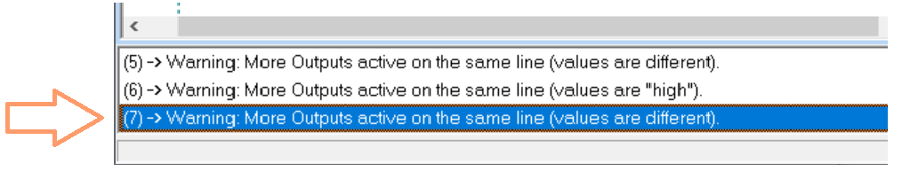
In the following example, instead, an erroneous activation of the control lines results in a logical (and electrical) conflict on the output Left, that will show an Unknown value ('--'):

As visible in the figure, the simulator highlights the net involved in the conflict, changing its color in red and surrounding it with a dotted rectangle. Moreover, an inherent message will be readable at the bottom of the window:
An example of usage of the bus-type tri-state buffers follows.

In the example above 8-bit busses are employed. In this screen-shot, the 8-bit data on IN_L is passed through the tri-state buffers chain, reaching the output Left, Center and Right. We could repeat the same observations done before.

In the example above, EN_L and EN inputs are not set, so the outputs LEFT and Center show the Hi-Z state. Instead, EN_R is set, so the output Right copies the data coming from IN_R.
Now, all the output components can display the 'Hi-Z' state. Here a few examples regarding Test LEDs, Test Points and Seven-segment displays:

In the figure a), from high to low, the Test LEDs show the states '1', 'Hi-Z' and '0'. The Test Points example b) displays 'Hi-Z' and '1' state. The undecoded-type seven-segment displays c), from left to right, show the segments 'f', 'a' and 'b' at '0', '1' and 'Hi-Z'. The two decoded-type seven-segment displays d) show the character 'F' and the 'Hi-Z' representation.
The internal global rule checker has been updated to support the bidirectional lines and tri-state buffers. For instance, the following connection is incompatible and it is signalled and the simulation inhibited:

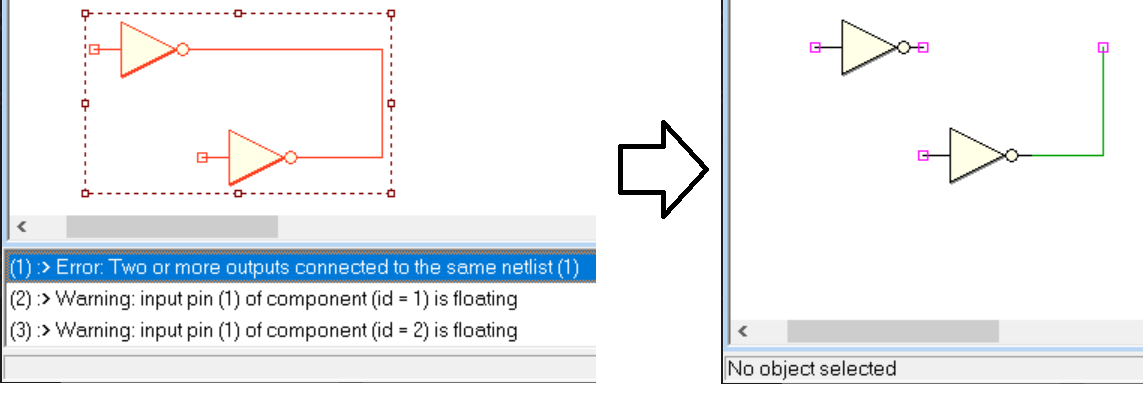
Moreover, now the internal global rule checker reveals also the nets with no component attached (i.e. nets that include only Wires, Busses, Splitter and Taps), signalling with a Warning that the associated netlist is 'unuseful' and 'floating'.
CBE Symbol Editor
The introduction of tri-state components lead to a modification of the CBE ('Circuit Block Element') functionalities and of the CBE editor. Besides the Input and Output PINs, now the Tool Bar of the CBE editor shows also the Bidirectional PINs:
In the next example, a CBE includes a simple NOT, that drives a 'normal' Output PIN, and a tri-state buffer that drives a Bidirectional PIN:

Note that a Bidirectional PIN is simply a PIN that can be connected either as Input or Output. Take into account that a CBE PIN is somehow 'virtual', given that it will disappear from the netlists. Indeed, the contents of the main file and of all the CBEs will be "flattened" in one netlist only, after the compilation (when done for the simulation or the VHDL exportation).
The symbol editor has been changed. Now, Input, Output and Bidirezional PINs can be placed anywhere, around the component symbol border. Before, the Input PINs should be placed on the left and top side of the symbol, and the Output PINs along the other sides. Since it did not make sense for the bidirectional pins to have such constraints, we made all PINs placeable anywhere.
File Version
The internal file format of the ".pbs" and ".cbe" files has changed (now: "1.033"). The change was necessary because of the addition of new components and new features to the FPGA/VHDL export module. The old files are readable by the new Deeds version, while files created by the current version are not compatible with the older ones.
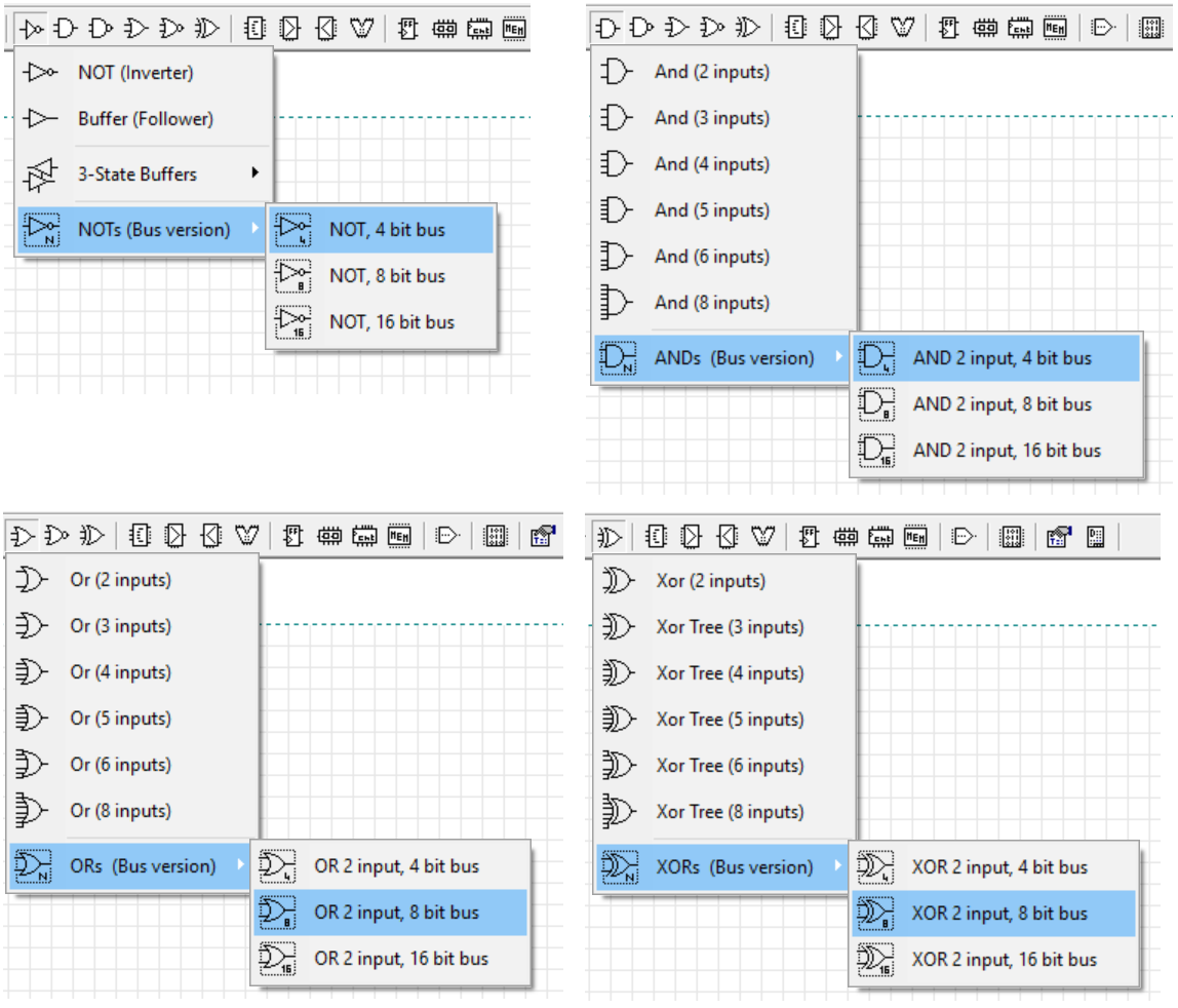
Bus-type NOTs, ANDs, ORs and XORs
Bus-type NOTs, ANDs, ORs and XORs have been added to the component library (size of 4, 8 and 16 bit). They are available under the respective icons, on the Component Tool Bar, as shown in the next figure:
The following figure shows an example of usage of the bus-type gates, employed into a simplified 8 bit Arithmetic and Logic Unit (embedded into a CBE):

New Counters
Two simple Up/Down 8-bit Counters with Enable have been added to the component library, one with normal pins, the other in bus version. Tested and working also on FPGA. Here an example of usage of these components:

Truncated Dialogs (bug fix)
On some installations of Windows 10, a few properties setting dialogs appeared to be cut off, and in fact they were unusable:
Now the problem has been solved. Thanks to Arkadi Poliakov and Slaith (Keith René Dugué) for the signaling and the tests concerning this problem:
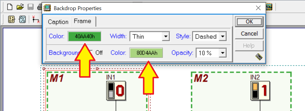
Color changing (bug fix)
In the last version it was impossible to change the colors of the elements of the Backdrop and TextBox components (due to the passage to Windows 10). Now the problem has been solved, using different controls, compatible with Windows 10. In the next figure, an example showing the Backdrop Properties Dialog with the new controls (pointed by the arrows):
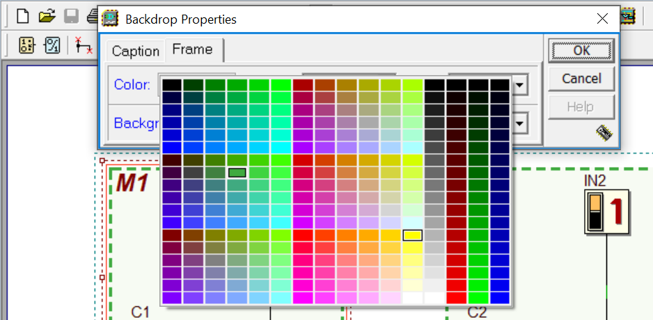
Clicking on this controls, a color palette is displayed, allowing the choice of the desidered color:
Symbol Editor (bug fix)
Now, if any command is active, and 'F7' is pressed to open the CBE Symbol Editor window, the active command is correctly terminated.
Warning/Error List (bug fix)
Now, the Warning/Error list at the bottom of the circuit editor is automatically hidden, if shown, when the circuit is modified:
Loading DMC8 project files (bug fix)
In case the user tried to load a DMC8 Project File ('.mce') provided for the 'basic' model, into the 'enhanced' one, a message warned correctly that it was not possible to load it. However, if visible, the 'Program Source Code' window remained visible, displaying improperly the file. Now the problem has been corrected.
Deeds-DcS (FPGA support)
New FPGA Boards Supported
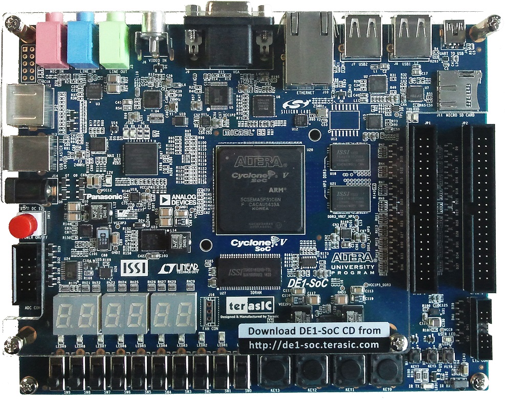
Support has been added for testing the Deeds projects on the Intel/Altera FPGA Board DE1-SoC:
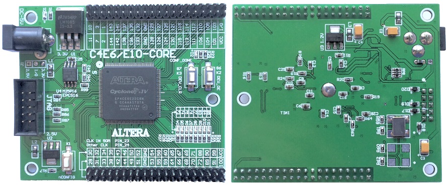
A few un-branded, entry-level FPGA Boards [available on eBay], have been added. For instance, the following one, based on the Intel/Altera chip Cyclone IV 'EP4CE6E22C8':
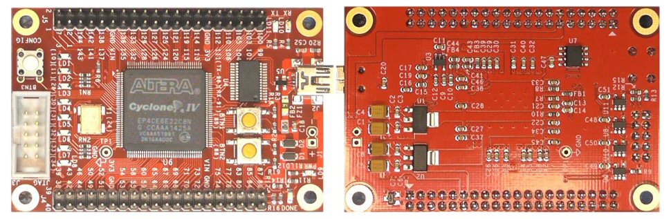
Another supported board is the one in the next figure; also this is based on the Cyclone IV 'EP4CE6E22C8' chip, too:
Instead, the following board is built around a CPLD component, the Intel/Altera MAX II 'EPM240T100C5N':
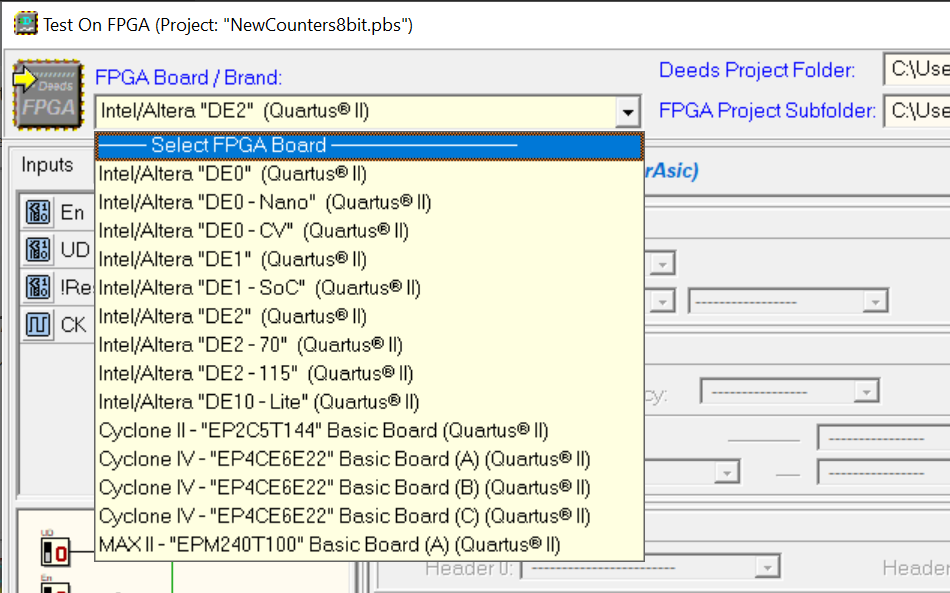
Here the complete list of the FPGA Boards supported by the current Deeds version:
Test on FPGA Expert: Header Pin Highlighting
The usability of the procedure to associate the Input/Output lines to the header pins of the FPGA Boards has been enhanced. Starting from the current version, a panel shows the top view layout of the header and highlights the selected pin. The following example shows the operations to associate an output to the 'Header 1' pin 'IO_031', whose physical position is highlighted by the small red arrow pointing to the pin '3' of the 'Header 1':
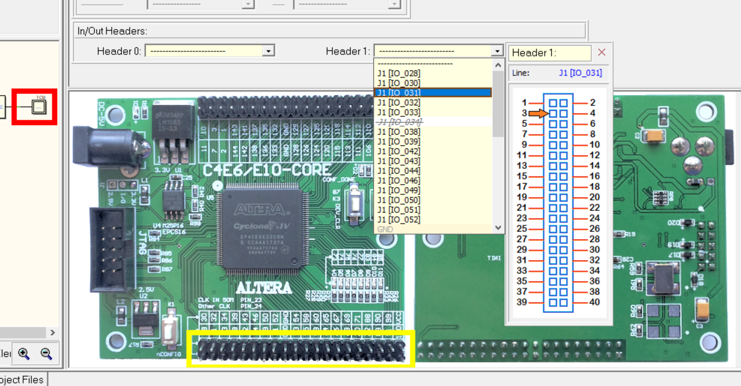
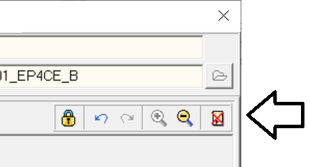
In this way, it will be simple to do external connections using the headers. Note that this new feature can be disabled (or re-enabled) by clicking on the little button in the upper-right side of the window (see the next figure):
Slow-clock Parameter control by Headers' Pin
A new management of the Slow-clock parameters has been added. It has been introduced because the entry-level cards comes normally without (or almost without) switches, push-buttons or LEDs. So we added the possibility to use, for all the supported FPGA Boards, the headers' pins as controls for the Slow-clock setting.
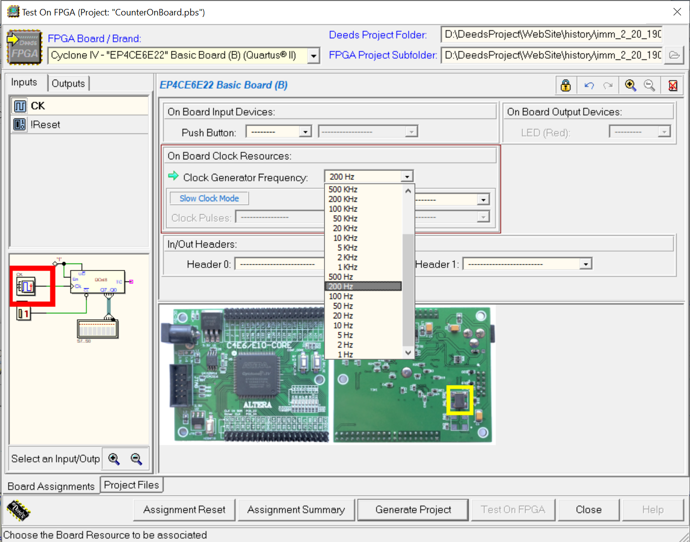
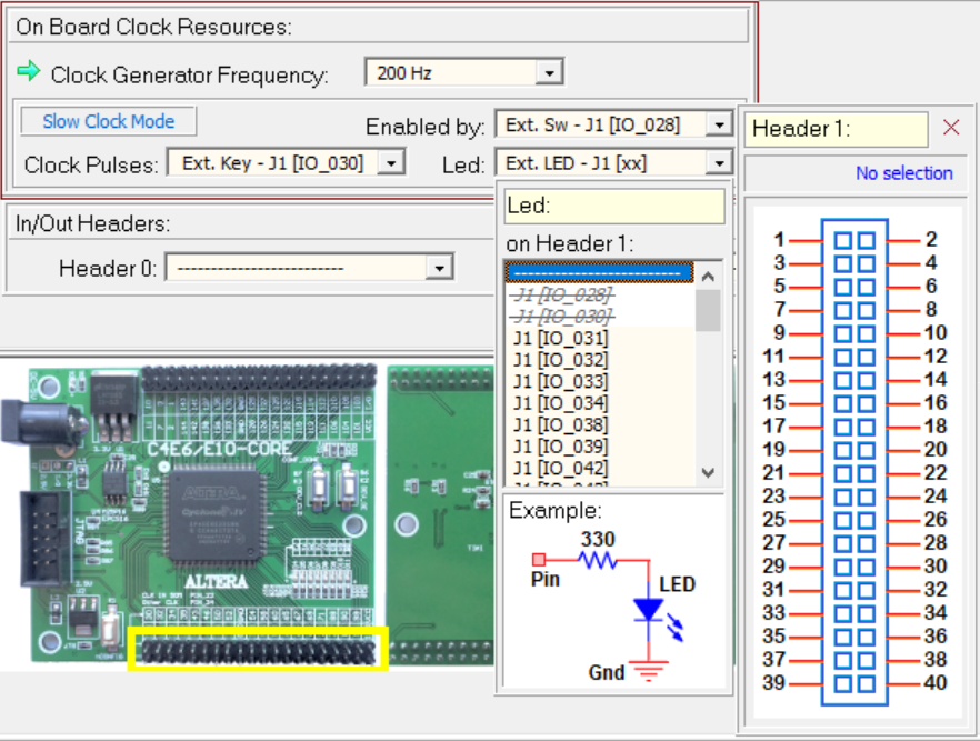
Let's explain the new feature with an example. Here a simple 8-bit binary counter that we want to experiment on one the Cyclone IV 'EP4CE6E22C8' boards:

We open the 'Test on FPGA' dialog and, first, we set the associations for the reset button and the 8 counter output (the board has two push-button and 8 LEDs available). Then, we try to configure the clock parameters, starting with the nominal clock frequency, that we set to 200 Hz.
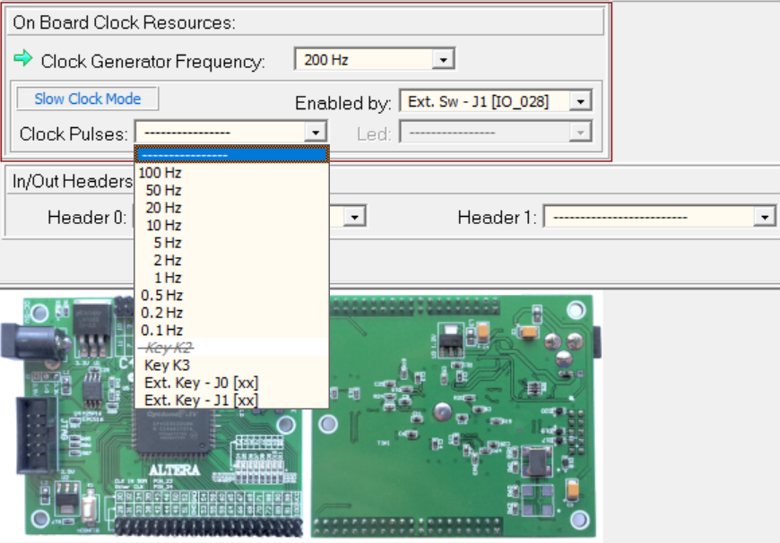
Now we want to set the Slow-clock parameters, and we start choosing a switch that will permit to commutate, at run-time, between the 'normal' clock and the Slow Clock debug feature.
Unfortunately, this simple FPGA board lacks of such type of resources. Deeds allows to use a pin of the headers, as evidenced by the drop-down list in the 'Enabled by' field:
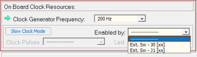
For instance, the string 'Ext. Sw - J1[xx]' abbreviates 'External Switch on Header J1, on a pin to be defined'. Then we click on this item, obtaining the following scenario:
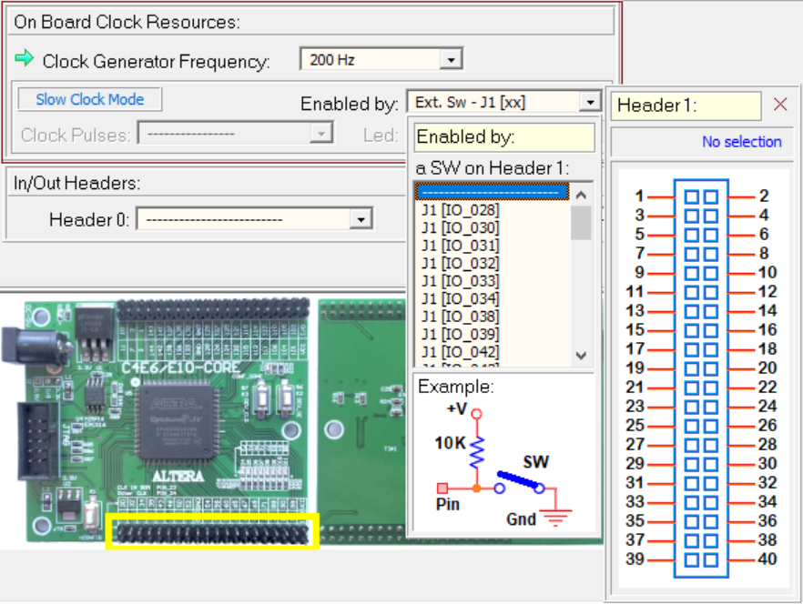
We can choose the desired pin on the header, while the schematic suggests to us how to connect the switch to the pin. Note that a debugger circuit is added to our project, behind the scenes; it is not visible, but it takes into account, among other things, the 'debouncing' of the switch and button used to control the Slow-clock parameters.
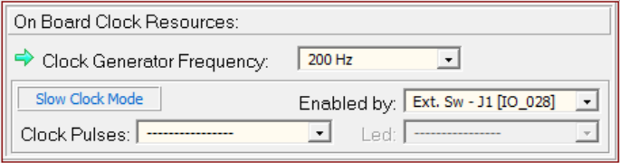
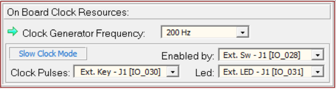
After having defined the pin, the 'Enabled by' field will show the setting:
Now it's time to define how to pulse the Slow-clock for debugging/testing our circuit. As visible in the next figure, we could:
- Pulse it automatically (choosing a frequency ranging from 100Hz to 0.1Hz),
- Define a push-button ('Key K3' is available), to pulse the clock manually,
- Connect an external push-button to a pin of one of the available headers.
We select the last option in the list box. Now, once again, we can choose the desired pin, while receiving a suggestion about the circuit needed to connect the external push-button that we'll use to pulse manually the clock, as shown in the next figure:
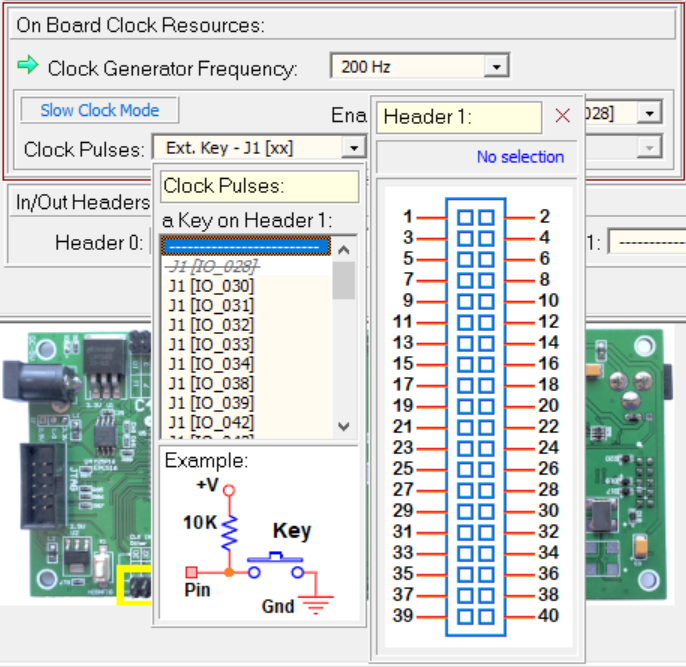
Remember that the 'debouncing' of the button is done automatically by the debugger circuit that acts behind the scenes, as seen before. After the click on the pin item, the 'Clock Pulses' field will appear as follows:
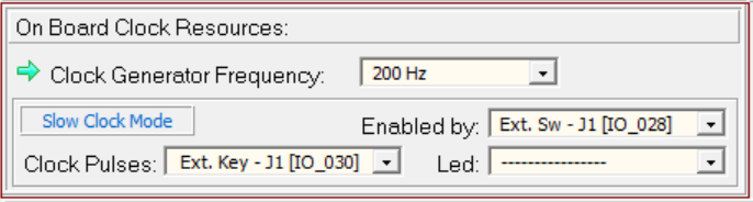
The remaining step consists in the connection of an external LED. This LED is used by the internal hidden debugger to visualize the clock pulses. As visible in the next figure, all the LEDs available on the board are already in use, so we need to select, once again, a pin of the available headers:
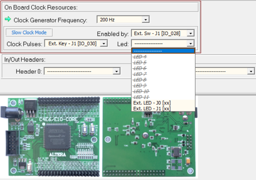
After a click on the last row of the list box, we'll see the following panels:
As before, we'll select the desired pin of the header, connecting the LED according to the schematic suggested by the figure. Finally, we obtain the setting:
Tri-state and Bidirectional Buffers inside FPGA
Tri-state components are regularly exported in VHDL. The FPGA compiler (i.e. Quartus II) will substitute the tri-state logic with an equivalent combinational network, if tri-state buffers are not elements included into the architecture of the FPGAs in use. Quartus II builds the substitution considering that a floating input, i.e. connected to a line in high-impedance, will read an high level.
Tri-state Buffers on FPGA Pins
At the moment, it isn't possible to configure, in a Deeds project, an FPGA pin as 'bidirectional'. However, exporting of a tri-state buffer on a FPGA pin is straightforward. Consider the following example:

The output shows, during the simulation, the capability to assume the high-impedance state. When exported to an FPGA board, the compiler will generate a tri-state buffer on the output pin, as expected (figures from Quartus II):
Intel/Altera-DE0, setting (bug fix)
In the 'Test on FPGA' dialog, in relation to the Intel/Altera-DE0 board: when defining the switch to enable the Slow-clock Mode, this ComboBox appeared empty. Now the problem has been solved.
Changes in VHDL renaming of Finite State Machines (bug fix)
In the previous versions, to be sure that Finite State Machines had unique names, their names are renamed and enumerated automatically, adding a postfix to the original name. Starting from the current version, the postfix has been substituted with a prefix. This to avoid problems with the VHDL naming rules and the maximum number of significant characters of VHDL identifiers. For example, a file named 'MyFile.fsm' is converted to a VHDL file with the name 'Fsm3_MyFile.vhd' ('Fsm_' has been prefixed to the original name, with the addition of a ordinal number).
Moreover, thanks to the report of William Samuel Frau, a bug in the VHDL exportation of a Finite State Machine has been solved. If its file name contained one or more spaces, or in general it was not VHDL-compliant, in the VHDL PORT MAPPING of the component, the file name appeared in the original version (not converted in VHDL-compliant form) and the compilation gave an error (the problem has been fixed).
'Test on FPGA' dialog: index auto-increment (bug fix)
In the 'Test on FPGA' dialog, index auto-increment was uncorreclty enabled for seven-segment display. Now the bug has been fixed.
Bus-type MUX components (bug fix)
Fixed the VHDL names of the BUS-type MUX components. Thanks to William Samuel Frau for the error report.
Launch of Quartus II (bug fix)
Fixed a bug related to the launch of Quartus II, when an alternative version of the tool was selected in the dialog "Ready to Test on FPGA" (see the next figure).
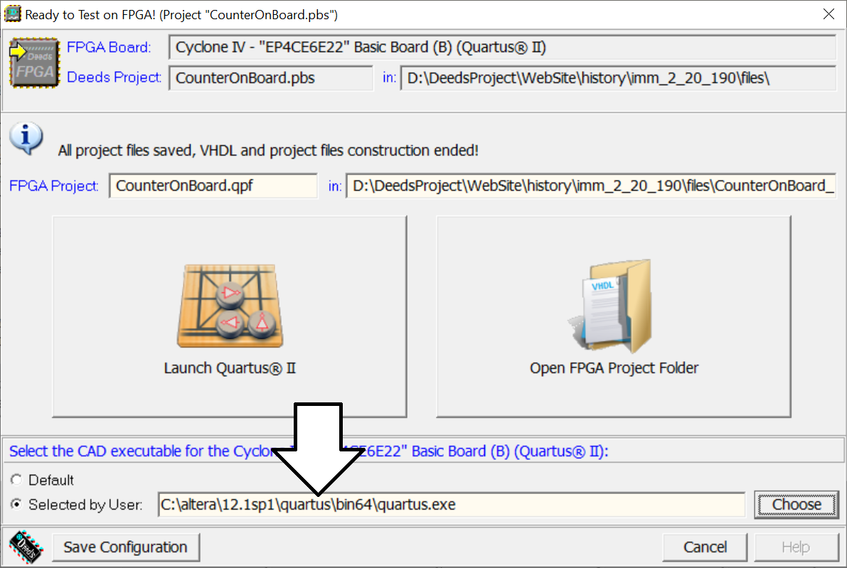
If the file path contained spaces in the directory names, Quartus II could not find the file. Now the problem is solved.
Deeds-DcS (Simulation By Animation)
Input Components and Initial Unknown Value
Following the suggestion by Arkadi Poliakov, we have implemented a new feature for the Input Switch component, usable in all the simulation modes ('By Animation' and 'Timing Diagram'):
Now it can generate a temporary 'Unknown' value on simulation begin, useful for testing the initial behavior of a network. This functionality, for now, is implemented for this component only. From the point of view of the VHDL export, it behaves like a normal entry.
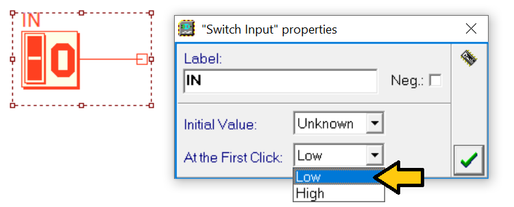
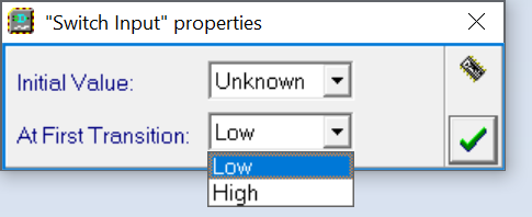
In the 'Switch Input' properties dialog, now it is possible to define an initial value 'Unknown' (in addition to 'Low' and 'High'):
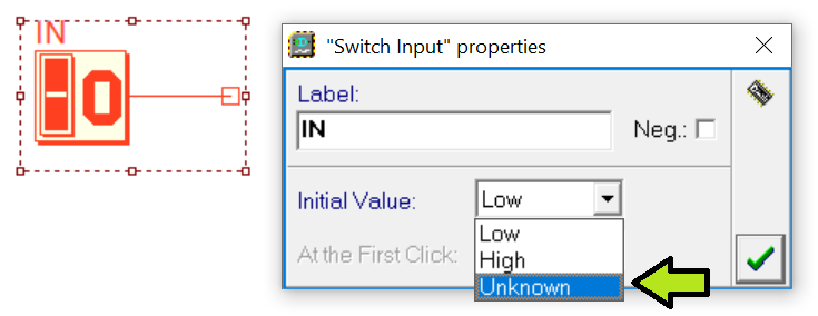
By selecting 'Unknown', the field below is activated. This field allows you to choose the value assumed by the input 'at the first click' on the component, after the initial value 'Unknown':
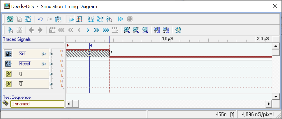
Consider the example in the next figure. Once the simulation 'By Animation' has started, the input 'Set' appears 'Unknown', as well as the outputs of the network (a):

At the first click on the 'Set' input (b), its value assumes the value set by the user. From this moment on, the input will alternately assume the values 'Low' and 'High', at every mouse click, as usual.
The behavior of this component, regarding the timing diagram simulation, is described just below.
Warning Messages (bug fix)
During the simulation 'By Animation', when a problem occurs, a message is added in the bottom box and the object is highlighted in the schematic, making a selection rectangle appear that includes all of them. See the example below:

In previous versions this highlighting selection could be rather annoying, because the last one remained visible, while continuing the simulation. Now, just at the next mouse click on the schematic, the selection is hidden. To review a previous highlighted selection, the user must simply click on the error/warning message of interest.
CBE Warning Messages and Error Highlighting (bug fix)
The display and highlighting of run-time problems, catched during the simulation and inside the Circuit Block Elements (CBE) showed various bugs. That problems seem to have been fixed in the current version, and the 'selection rectangle' is displayed correctly in the main schematic and in the CBE schematics opened into the CBEViewers.
In the following basic example, a Tri-state buffer has been enclosed into a CBE, also this one used in the main schematic. The activation of both the Tri-state enable lines (C1 and C2) originates a logical conflict on the network connected to the output line OUT. As visible in the figure, the run-time problem is correctly highlighted either in the main schematic and in each CBE Viewer:

Decoders (bug fix)
In the previous version, the Decoder components, when the inputs were 'Unknown', generated 'Low' on the outputs, instead of 'Unknown' as expected. This behavior has been corrected.
List Out of Bound Error (bug fix)
Fixed a bug: simulating a network, after having drawed it and not yet saved, rised a 'List Out of Bound Error'. By saving and reloading the file, the problem no longer appeared.
Erroneous opening of the CBE Symbol Editor (bug fix)
The CBE Symbol Editor has been opened, even if we were not editing a CBE, on pressing the 'F7' shortcut. Now the short-cut 'F7' is not effective, unless the open file is properly a CBE, as expected.
Clock Animation Button (bug fix)
Fixed a bug regarding the simulation 'By Animation' of a network containing a DMC8 Microcomputer. When a software breakpoint was reached, the clock stopped regularly, but the Clock Animation Button, in the Object Code Window, was not updated as it should be.
Erroneous opening of the Timing Diagram Window (bug fix)
If we were in simulation 'By Animation', by pressing the shortcut 'F8', the Timing Diagram Window was activated, bringing the system to an inconsistent state. Now the shortcut 'F8' is correctly disabled while in simulation 'By Animation'.
Deeds-DcS (Timing Diagram)
Input Components and Initial Unknown Value
As described before, the functionality of the Input Switch component has been changed. Now, it can generate an initially 'Unknown' value also in the 'Timing Diagram Simulation' mode. In a previous example, the input '!Set' was set to an initial 'Unknown' value for the simulation 'By Animation' mode. Now we set a similar property in the Timing Diagram Window, by clicking on the '!Set' track and opening the initial value editor (see the big arrow in the next figure):

The dialog allows to define an 'Unknown' as initial value of the track:
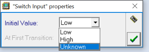
Selecting this value will activate the field 'At First Transition' which is immediately below:
This field allows you to choose the value assumed by the input at the first transition that we'll add, in the usual graphical mode, by clicking on the track itself:
This transition from 'Unknown' to the chosen value, could be moved as the other transitions.
Default Time Scale
Previously, opening the timing diagram window without a test sequence already defined, the time scale appeared maximized at picoseconds level. Now the time scale is defined to display at least 50 nS on the horizontal scale, in the absence of defined transitions. Instead, in their presence, for a time duration longer of this time, the scale is calculated by executing an automatic 'Fit View' command.
Memory Usage Meter
Now, during the Timing Diagram simulation, the system checks in advance the memory availability and stops the simulation before a possible program crash could happen. On the top right of the Timing Diagram, a meter is visible during the simulation. It displays the current available memory (see the figure below):
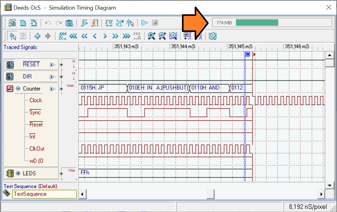
However, the memory meter is initially hidden, until the memory usage reaches about the 10% of the available space. In this way, when simulating little circuits, the meter is not shown.
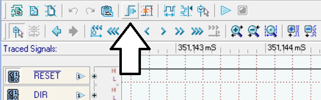
'Edit Edges' button (bug fix)
In the previous version, the 'Edit Edges' button was erroneously almost always grayed. To edit a track was necessary to click on the track itself. The problem has been solved.
Sub-title (bug fix)
Fixed a bug of the Sequence Editor Undo in the Timing Diagram window, which concerned the input components of type Array and Hex.
 Deeds-McE
 No correction in this release
 Deeds-FsM
 No correction in this release
Deeds-DcS, Deeds-FsM, Deeds-McE
This version of Deeds had been tested under Windows 10 (32 and 64 bit). We recommend that you do not install it in previous versions of Windows.
