![]() Deeds-DcS (Editor)
Deeds-DcS (Editor)
The main novelty of this latest version is the ability to build components that can be reused in another circuit. The new "Circuit Block Elements" (CBE) components are user-defined in terms of schematics, enclosed within a component symbol. In the next figure, the schematic of a decoder 6 to 64 lines, is enclosed within a CBE.

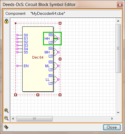
A CBE component is saved with the extension ".cbe" (unlike the ordinary ".pbs"). A CBEfile contains, in addition to the circuit database, also the description of the component symbol. This is user-defined through the Symbol Editor (see the next figure), integrated into the Deeds-DcS.
After saving the ".cbe"file, it becomes available to be inserted into an ordinary schematic (".pbs"). In the following figure, the example shows the "Dec 64" CBE, connected as a normal library component: a binary counter drives the decoder inputs, and its outputs are connected to 64 LEDs:

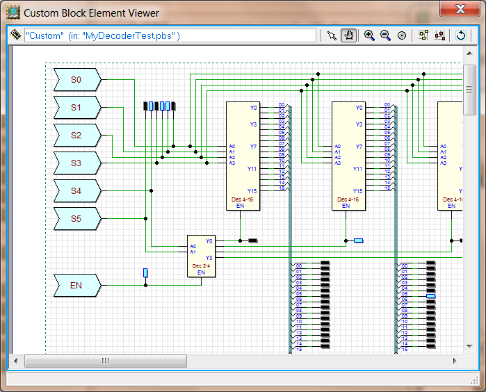
During the simulation "By Animation", you can observe also the activity of the CBE internals, simply with a click on the CBE component. The CBE Viewer will show, animated, the internal schematic:
At this moment, the CBE can not contain other CBE components; however, it may contain any other component, such as Finite State Machines and/or a Microcomputer.
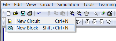
As you see in the figure, starting with this version, you can create two kinds of file. "New Circuit" will create a circuit ".pbs" file (as in the previous versions), and "New Block" , instead, will generate an empty ".cbe" file :
When you create a new CBE file, the Symbol Editor window is automatically opened, close to the main window:
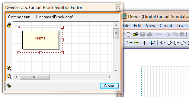
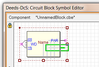
By now, in the Symbol Editor, it is possible only to resize the component rectangle, using the mouse, or change the Name that appears in the middle of it, but no pin is there yet. A new pin is created (and placed on the bounds of the rectangle) when you add a Component Pin to the schematic. In the next figure, the menu of the available Input Pins and Output Pins are shown:
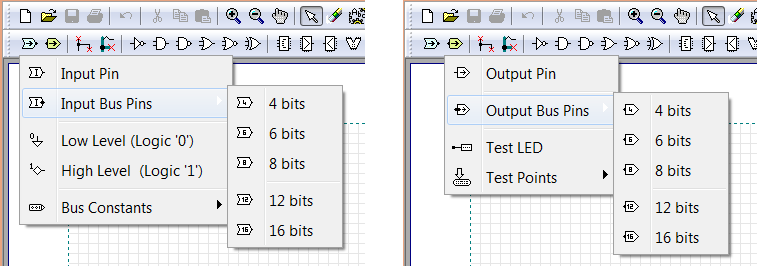
A "Pin" can be Single-Wire or Multi-Wire ("Bus"). From the menu, we get a Bus Input Pin of 16 bits, and insert it, as a normal component, in the schematic. As you see in the next figure, we are asked to give a Name to the Pin, and to write a Description Label. Note that it is necessary to name differently all the used Pins (the code does this check for us).

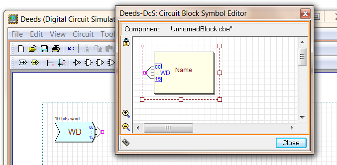
As soon as you close the properties dialog, the schematic editor will show the Component Pin with the highlighted "WD" name, ready to be connected to the internal parts of the CBE . Furthermore, the new Bus Pin appears on the Symbol Editor (as shown in the following figure):
In a similar way, now we insert in the circuit a single-wire Output Pin, giving it the name PAR:
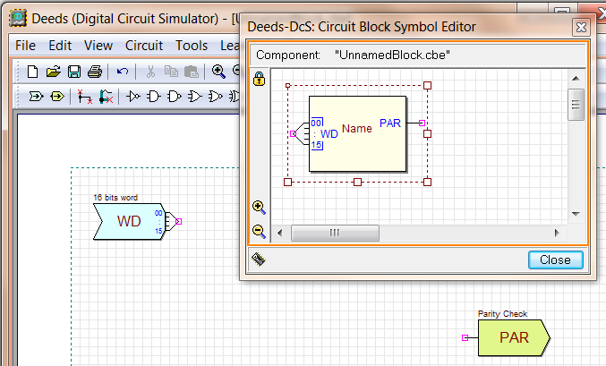
By default, the Input Pins are placed on the left side of the symbol (but you can also move them on the upper side), while the Output Pins will appear on the right side (moveable on the bottom side). In the next figure, you see the placement options offered by the Symbol Editor , when you try to drag and drop the pin with the mouse:
Then, we complete the CBE Component Symbol: by clicking on the "Name" in the middle of the rectangle, will appear the dialog window "Edit Component Name and Hint Message" . We assign"Parity Gen" as Name, and "Parity Generator (16 bits)" as Hint Message (see the figure):

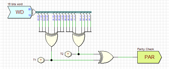
Now is the time to draw the schematic of the internal circuit. This short example proposes the drawing of a simple EXOR tree, generating the parity of the 16 bits word received at the input. Two test points (T1 and T2 ), added to the circuit, will help us later, during the simulation:
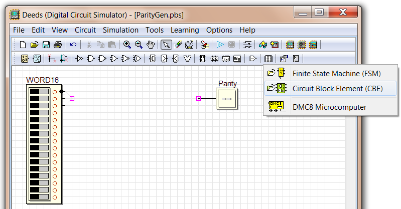
After saving the file with the name "ParityGen.cbe" , we'll go to insert the new component into another schematics. We create a new circuit file (".pbs" ), as you see in the following figure. For sake of simplicity, we insert in the schematic only a 16-switches Input Component, and a binary Output. Then, we insert the Circuit Block Element just defined, opening the Custom Component menu:
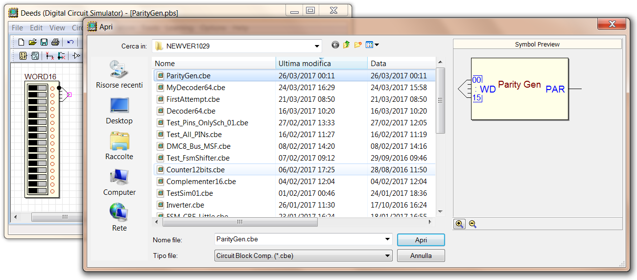
The following dialog will appear. We select the CBE saved before, "ParityGen.cbe" (theSymbol Preview helps us in choosing the right CBE ):
At the insertion of the CBE, we assign a Label to the component:
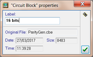
The Label (in this example "16 bits") will appear immediately under the name of the component, at the center of the rectangle (see the next figure). After the insertion of the CBE, we complete the circuit with a few bus and wire segments, and we save it:
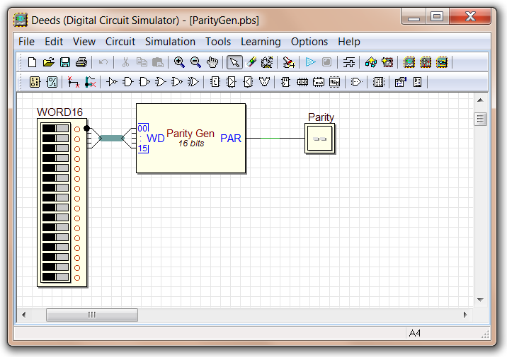
It is possible to simulate the circuit (now with the Interactive Simulation). At first glance, it could seem impossible to observe the interior of the block. Instead, just click on the CBE (during the simulation) and you'll open a window that will allow you to observe also the circuit inside the CBE:

The Test Points (T1 and T2), added before to the circuit, help us to display the values of the lines, during the simulation (both in animation and in timing diagram modes).
The Custom Block Element Viewer allows a minimal set of commands, as Pan, Zoom In, Zoom Out, View All, identical to the ones of the main mindow circuit cditor. For instance, it is possible to save the current view on the clipboard, or as an image file ("BMP", "PNG"):

Moreover, the right-most button  , if set, allows the automatic re-opening of the Custom Block Element Viewer when you restart the simulation.
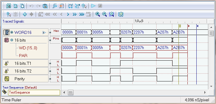
The following figure shows an example of timing simulation of the circuit:
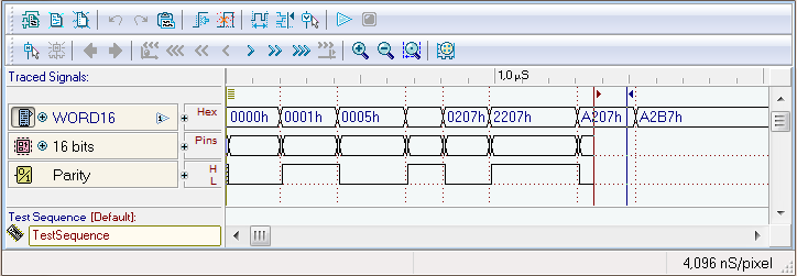
The CBE appears as a track labeled as "16 bits" (the label assigned before). By clicking on its Track Label, the following context menu will show:
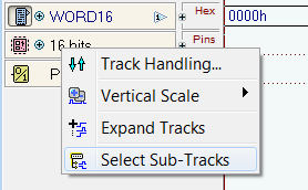
Clicking on the menu item "Select Sub-Tracks", we'll open the Sub-Tracks Dialog, where are listed all the Input and Output pins of the CBE component:
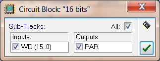
We have only two pins: we select all the two (just to practice, because these signals, in the present example, are already displayed by other components in the diagram). Closing the dialog, they will show up in the timing diagram, as sub-tracks of the "16 bits" main track :
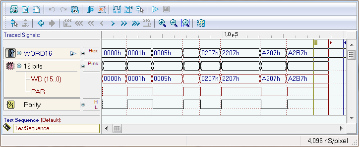
By default, the internals of a CBE are hidden in the Timing Diagram. Before running the simulation, you can choose the signals to be displayed. By clicking on its Track Label, the context menu will appear, as seen before. This time, we select "Track Handling", to open the Track Handling Dialog:
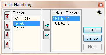
The Track Handling Dialog, introduced with the current version, allows to move up or move down the selected track (using the arrows on the left side) and to Hide or Show all the output tracks (it makes no sense to hide the Input tracks). We click on the horizontal arrows to add the hidden tracks to the visible Track List; then, using the vertical arrows, we move the Parity track below T1 and T2:
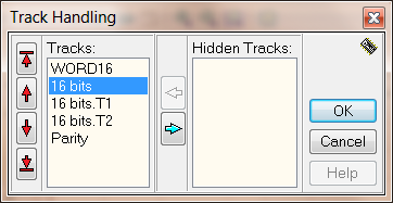
Finally, the resulting timing diagram simulation will have the following aspect:
The size and aspect of a few Input/Output components have been reduced, to better fit the available space and make them look less bulky. The new "Switch", "Push-button", and "One bit Display" are shown in the following example (compared with the old ones):

Component library has been extended, mainly with the addition of several 16-bits devices, but also with a couple of powerful Arithmetic and Logic Units. Here, in detail, all the novelties:
![]() Input Dip-Switches
Input Dip-Switches
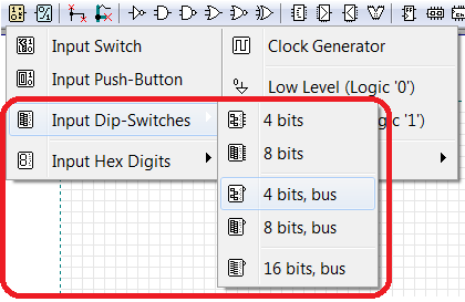
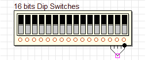
In addition to the 4 and 8-bits versions ("normal" o "bus"), now a 16-bits Dip-Switches is available (only with the "bus" connection):
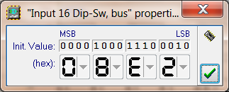
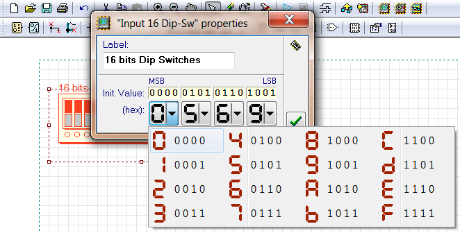
Moreover, the Input Dip-Switches Properties Dialog is slightly changed. You'll change the Initial Default Value of an Input Dip-Switches component by clicking on the Down Arrow of the Hex Buttons , as you see in the next figure:
![]() Input Hex Digit
Input Hex Digit
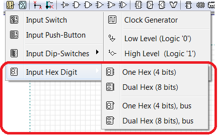
These input components are new, and available in the 4-bits 8-bits version ( "normal" o "bus" ):

Input Hex Digit components are substantially identical to the Input Dip-Switches but, during the Simulation by Animation, they allow to change the value of a group of 4 bits at a time (as Hex Digit), with a click on the component (see the next figure):
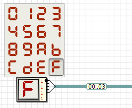
The Initial Default Value of an Input Hex Digit component can be changed by the Input Hex Digit Properties Dialog, almost identical to the one of the Input Dip-Switches.
Special thanks to Jérôme Lehuen for the suggestion to insert this kind of component in the library.
![]() Bus Constants
Bus Constants
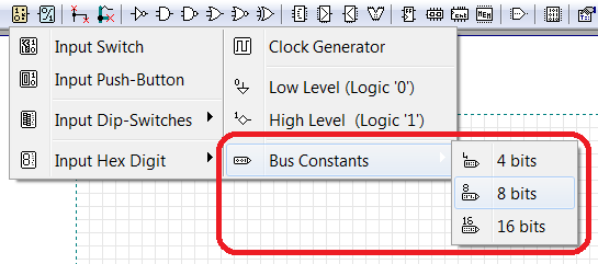
The Bus Constants defines a set of binary constant values to be applied to a bus. Three sizes are available: 4, 8 and 16 bits:

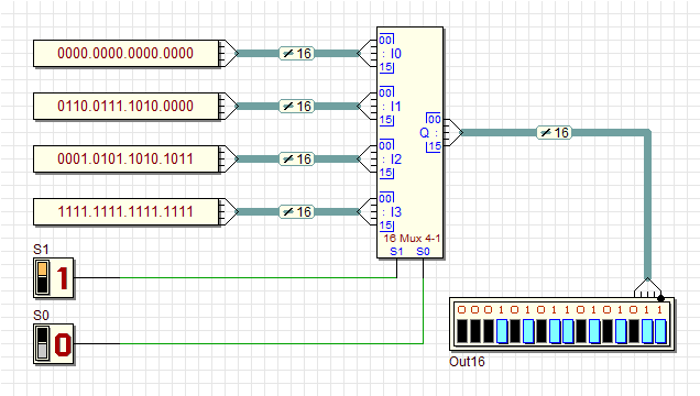
Here an example of usage: a Bus Multiplex selects one 16-bits value, among the four available:
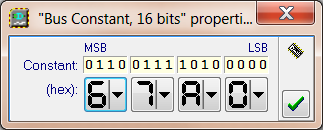
To define the value of the binary constant, the Bus Constant Properties Dialog is available (similar to the others seen before):
![]() Output LED Arrays
Output LED Arrays
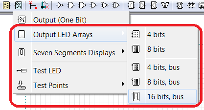
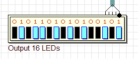
In addition to the 4and 8-bits versions ( "normal" o "bus"), now we have available also a 16-bits LED Array ("bus"connected):
![]() TestPoints
TestPoints
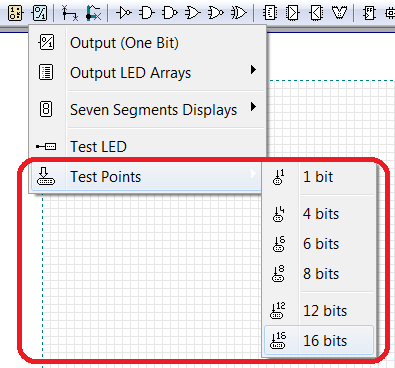
Test Points have been introduced to allow displaying of signals during the simulation, without having to insert bulky Output Components into the schematics. Test Points are visible in the Timing Diagram (note, the Test LEDs are not). Also, they are useful to display and/or time tracing CBE internal signals. The available Test Points (see the menu above) have the following shapes:

![]() Complementers (in: Arithmetic Circuits)
Complementers (in: Arithmetic Circuits)
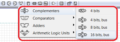
Next to the 8-bits bus version of the Complementer , the 4 and 16-bits size have been added:

We remember the function of the two control inputs Cpl and Two:
Cpl |
Two |
function |
'0' |
'x' |
Output = Input (as is) |
'1' |
'0' |
Output = Ones' Complement of Input |
'1' |
'1' |
Output = Two's Complement of Input |
![]() Magnitude Comparators (in: Arithmetic Circuits)
Magnitude Comparators (in: Arithmetic Circuits)
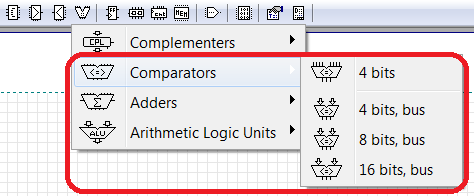
Similarly, we added the 4 and 16-bits versions to the Comparator series:

![]() Adders (in: Arithmetic Circuits)
Adders (in: Arithmetic Circuits)
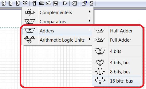
Besides the enhancement of the 4 and 16-bits versions to the Adder series, we added two simple components, the Half Adder and the Full Adder:

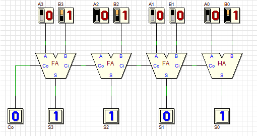
Here an example of a simple 4 bits ripple carry adder, using Full and Half Adders:
![]() Arithmetic and Logic Units (ALUs) (in: Arithmetic Circuits)
Arithmetic and Logic Units (ALUs) (in: Arithmetic Circuits)
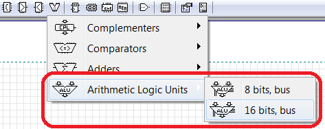
The two new ALU components are the following ( 8 bits and 16 bits):

Operands and Results:
ALU 8 : A = A07..A00, B =B07..B00, F = F07..F00
ALU 16: A = A15..A00, B = B15..B00, F= F15..F00
Ci: Carry Input; Co: Carry Output; Z: Zero Condition; V: Overflow Condition
S4 .. S0 |
Function |
Notes |
00000 |
F = 0 |
|
00001 |
F = +1 |
|
00010 |
F = -1 |
|
00011 |
F = - Negative Minimum |
-215 (16-bits version), or -27 (8-bits version) |
00100 |
F = A |
|
00101 |
F = B |
|
00110 |
F = not A |
Ones' complement of A |
00111 |
F = not B |
Ones' complement of B |
01000 |
F = A and B |
(Bitwise) |
01001 |
F = A and (not B) |
(Bitwise) |
01010 |
F = (not A) and B |
(Bitwise) |
01011 |
F = A nor B |
(Bitwise) |
01100 |
F = A or B |
(Bitwise) |
01101 |
F = A or (not B) |
(Bitwise) |
01110 |
F = (not A) or B |
(Bitwise) |
01111 |
F = A nand B |
(Bitwise) |
10000 |
F = A exor B |
(Bitwise) |
10001 |
F = not (A exor B) |
(Bitwise) |
10010 |
F = (not A) + 1 |
Two's Complement of A |
10011 |
F = (not B) + 1 |
Two's Complement of B |
10100 |
F = A + 1 |
Increment of A |
10101 |
F = B + 1 |
Increment of B |
10110 |
F = A - 1 |
Decrement of A |
10111 |
F = B - 1 |
Decrement of B |
11000 |
F = A + B |
Addition |
11001 |
F = A + B + Ci |
Addition, with carry input |
11010 |
F = Sat(A + B) |
Addition, with saturation |
11011 |
F = A - B |
Subtraction |
11100 |
F = A - B - Ci |
Subtraction, with borrow input |
11101 |
F = Sat(A - B) |
Subtraction, with saturation |
11110 |
F = B - A |
Reverse subtraction |
11111 |
F = B - A - Ci |
Reverse subtraction, with borrow input |
![]() Registers
Registers
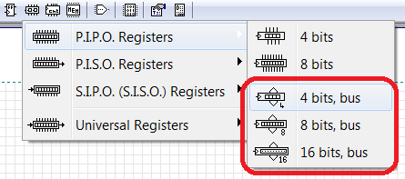
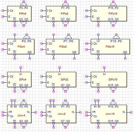
The Register Components have been all enhanced, completing all the 4 and 16-bits bus versions:
![]() Counters
Counters
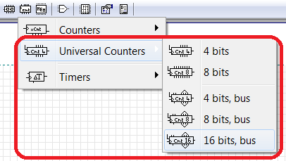
Also the Counter Components have been all enhanced, completing the series from 4-bits to the 16-bits bus versions:

![]() RAMs(Asynchronous) Memories
RAMs(Asynchronous) Memories

The Asynchronous RAM components are the same of the previous versions, denominated simply RAMs (now, we have also the synchronous types, see below).
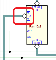
Note that a bug of the asynchronous RAM 16x8 has been fixed (thanks to Miles Smith for the first report about it). The size of the address bus pin (see the figure) has been corrected (in spite of the pin caption [A3..A0] , the pin size resulted, erroneously, of 8 bits).
![]() RAMs(Synchronous) Memories
RAMs(Synchronous) Memories

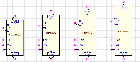
The Synchronous RAMs are a novelty of the present version. Here the available components with the storage cell of 8 bits :
And those with the cell of 16 bits:
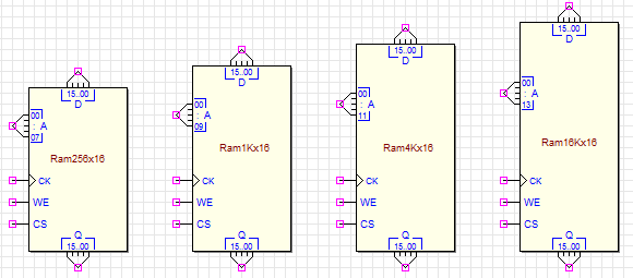
The synchronicity concerns only the write data operation. Reading is asynchronous. When the RAM is selected (CS = '1') and theWrite Enable (WE) is set to '1', data on the Input D is registered in the location addressed by A, and then appears on the Output Q.
![]() ROMs Memories
ROMs Memories

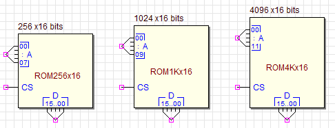
The novelty in the ROM components is represented by the 16 bits types:
Fixed a BUG regarding ROM programming: now the folder where a ".DRS" file has been opened/written is correctly memorized (even when reading, not only when saving files).
![]() Digital to Analog Converters
Digital to Analog Converters
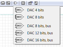
The Digital to Analog Converters (DAC) have been extended with the 12 and 16-bits (bus) types:

(At the moment, the DAC components cannot be exported to a FPGA board).
![]() Custom Components
Custom Components
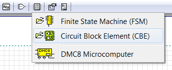
The existing Finite State Machine (FSM) components and theDMC8 Microcomputer have been grouped together with the new CBE components.
Now it is possible to export your Deeds project also onto the DE10-Lite FPGA board, by Altera® Corporation. Here the available boards, just giving a look to the window "Test On FPGA":
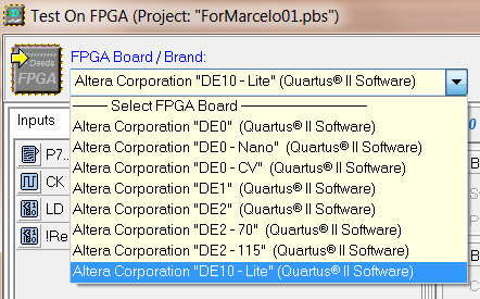
Special thanks again to Marcelo Dantas that suggested to support also the DE10-Lite board, and for helping us during beta testing of this new feature.
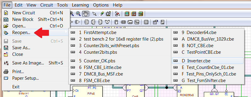
The "Recently Opened Files" registration method has changed. Now it is compatible "multi-instance ", i.e. all the opened Deeds-DcS instances will benefit of the same list of previously opened files, although opened from "siblings" instances. Moreover, now the list includes up to 16 entries, and the new menu item "Reopen" is positioned immediately under the "Open" item:
In the present version a new viewing mode has been added. You can activate it using the new "Schematics Only" command, available under the View menu:
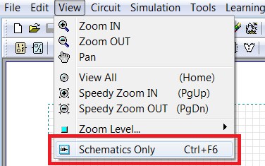
The new mode is also accessible with the short-cut <Ctrl> + F6 which acts in a toggle mode. <Escape> exits the command. This display mode allows to show a network hiding the Input/Output components: their symbols are replaced by a simplified drawing of the Input and Output terminations. The schematics created in this way are particularly useful for creating documentation suitable for the publication of articles and books.
The example below shows an arithmetic circuit: in the normal view (on the left side) and in "Schematics Only"mode (on the right side):
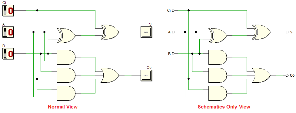
In "Schematics Only", the editor becomes read-only; simulation and VHDL and FPGA export are inhibited. Only the Zoom and Pan commands are active (by default, the last is activated automatically). The "Schematics Only" command closes any other one active at that time; moreover, it is inhibited if the simulation is active.
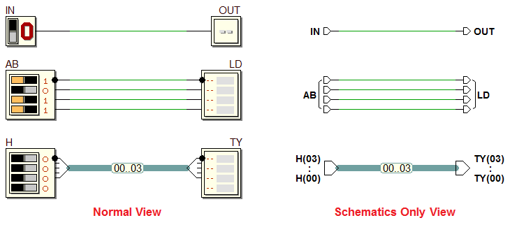
Much of the input and output components are enabled to be drawn into "Schematics Only" mode (even the "Test LED", but without showing a pin name, as they have none). Instead, the command does not change the graphics of the DACs and of the Seven Segment Displays. Some examples in the next two figures:

In the present version, two new options have been added to the Save Circuit Image Dialog: "Schematics Only" and "Show Unconnected":
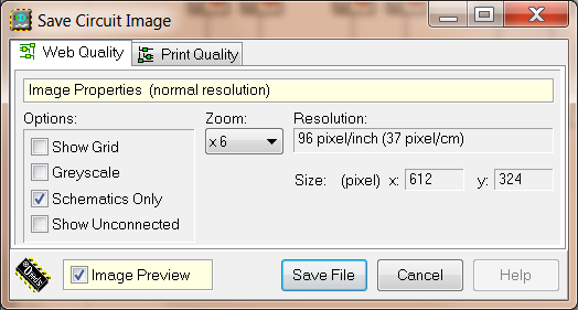
As you see in the next figure, the "Schematics Only" option allows to save an image with the Input/Output terminations modified as explained before:
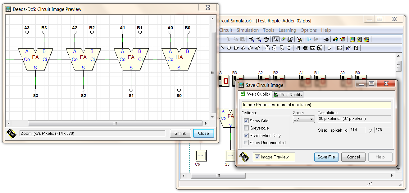
The "Show Unconnected" check box allows to include / not include, in the image, the highlighting of the unconnected pins (in the circuit editor, instead, this information is never hidden to the user). The following figure shows the effects of this option:

Now, in the Save Circuit Image Dialog, the Circuit Image Preview window is shown if the Image Preview Check Box is set:

Moreover, if this control is set, the Circuit Image Preview window will show automatically when the dialog will be reopened (the options settings are retained even if the image is not saved).
Labels at Component Insertion
Starting from the present version, the insertion of components that require the definition of an Identification Label or a Name, is immediately followed by the opening of the specific properties dialog, suggesting to assign the string to the component:
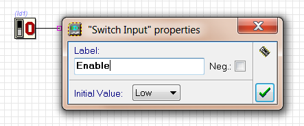
In addition to the simple components such as Switches, Push-buttons, etc., this is implemented also for the new Circuit Block Elements, the MSFs, theDMC8, the ROMs and the DACs.
Component Labels Compatibility
The Label of the components included in a circuit can be up to 31 characters. The allowed characters are letters (uppercase or lowercase), decimal digits, spaces, the symbols "-" and ".", the underscore "_" and all kinds of brackets. No other symbol is allowed, except the negation "!". In whatever position you introduce the negation "!", this will always be automatically moved before the other characters. If the negation "!" is inserted or deleted from the string, the negation check box is automatically marked consistently; if you click on the check box, the negation character is automatically added or deleted in the string. In the drawing, the negation will then be displayed as a horizontal bar above the label (see the example):

Note that, in the previous versions, the labels could contain any characters. A label previously assigned, containing characters not allowed, is still compatible. We suggest to delete those not allowed from any new or revised project, but it is not a problem if you leave them in place.
PIN Names (Custom Block Elements)
The name of a normal single-wire PIN can be composed of a maximum of three capital letters or numerical digits and cannot contain spaces, underscores or other symbols. It can be composed of numerical digits only. It may be preceded by the negation "!". The negation character is handled in the same way of the Component Labels. In the following example, the CBE has only two single wired PINs, named INP and !OUT.

The name of a multi-wired "bus" PIN can be composed of a maximum of TWO capital letters, and cannot contain spaces, symbols or numeric digits (this restriction is due to space limitations in the component symbol). The name of a bus-type PIN cannot be negated (the negation character is not accepted). In the following example, the CBE has two multi-wired input PINs, named CA and CB, and one multi-wired output PIN, named DD :

Custom Block Elements: Component Name and Hint Message
The Custom Block Element "Component Name" appears at the center of the Component Symbol and can be edited by clicking on it, in the Symbol Editor window (see the example in the next figure):
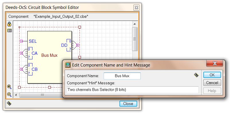
The name can contain letters (uppercase or lowercase), numerical digits, spaces, underscores "_", and the symbol "-". It can be composed entirely of numerical digits, and cannot be negated (the negation character "!" is not allowed).
In same dialog window, it is possible to edit also the "Hint Message". This is useful when a CBE component is inserted in a circuit: the message is displayed when moving the mouse cursor over it.
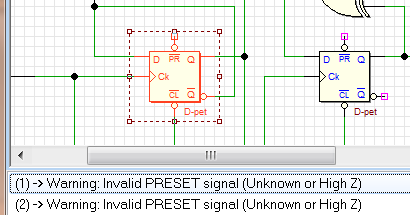
No more errors there, after the connection of the two preset inputs to the constant '1'(High):

In a similar way, the Enable input "En" (for those Flip-Flops that require it), must necessarily be connected. Regarding the Adders, now it isn't possible anymore to leave unconnected the input Cin.
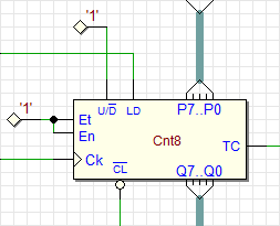
In a similar way, for the Counters, it is now necessary to connect the inputs Load ("LD"), Up/Down ("UD") and enable ("Et", "En"), to avoid failure when simulating:
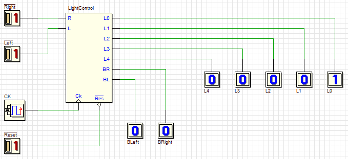
Consider, as an example, the following circuit, where we have inserted a FSM:
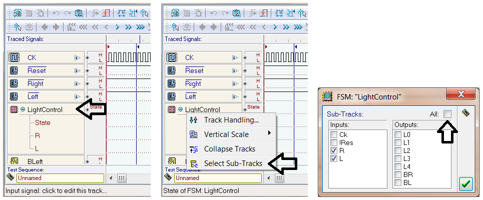
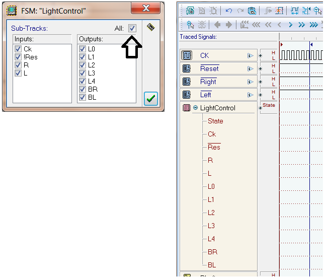
In the Timing Diagram, as highlighted in the next figure (on the left side), the FSM appears with the user-assigned name "LightControl": a few sub-tracks are already visible. If we click on the track name, the context menu will appear; clicking again on the item "Select Sub-Tracks", we open the Sub-Tracks Dialog. Starting from the current version, the "All" check box is present (see the figure):
Once selected, all the sub-tracks will appear:
The Sub-Tracks Dialog works with FSM components, with the DMC8 micro-computer and, now, with the custom CBE components. Note that we can select the desired sub-tracks only before starting the simulation.
The handling of the main tracks vertical position has changed: in addition to moving tracks downwards, or upwards, now we can also hide/show them. The previous commands have been replaced by only one, the "Track Handling", in the tracks context menu:
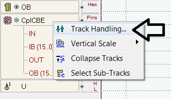
A click on this menu item will open the Track Handling Dialog:
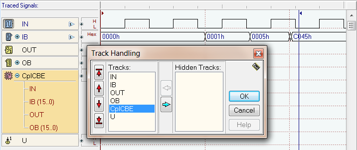
In the dialog will show one track selected: it is the one where we have activated the context menu. The track (as you see in the figure above) is also highlighted in the Timing Diagram.
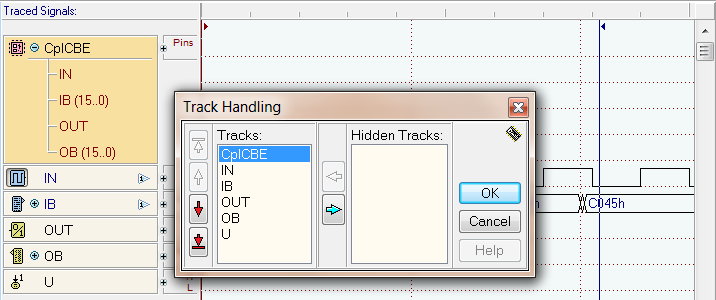
Using the red arrow buttons it is possible to move the selected track vertically:
 Move to top
  Move Up (one step)
  Move Down (one step)
  Move to bottom
For instance, after a click on the first button, the selected track movedon top:
Sometimes too many tracks can result in a Timing Diagram difficult to read, so it is possible to hide the tracks, by clicking on the green arrows, at the center of the dialog, as you see in the next figure:
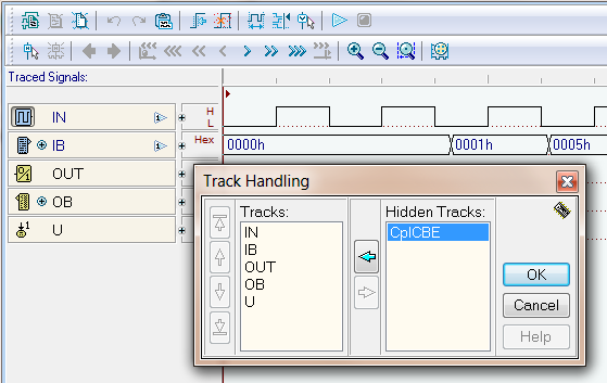
The tracks, related to the internal signals of a CBE, are initially hidden by default. All the available tracks will appear in the"Hidden Tracks" list box. Also in this case, we can show/hide the desired tracks only before starting the simulation. Note that you cannot hide an Input Track.
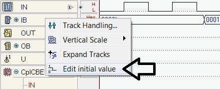
Fixed a bug: in the dialog of the initial value was possible to change thestart value of a track, even if the simulation was already started. We remember here that the dialog shows up by clicking on the "Edit InitialValue" menu item:
The contents of the dialog depend from the particular type of signal; here an example related to the "Input 16 dip-Switches":
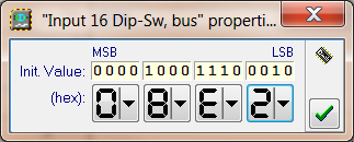
After the simulation is started, this dialog will appear grayed, looking like this:
