Pulse Width Modulator Component
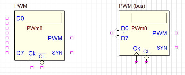
Two versions are available, with normal or bus inputs. Both versions have an 8-bit input data size (see the next figure).
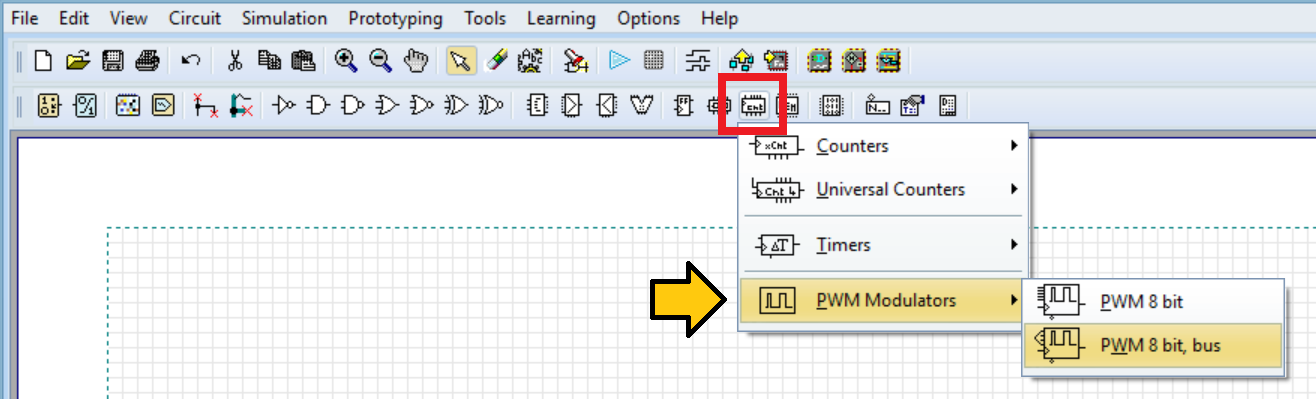
The following figure shows that the counters group contains the PWM components.
The test circuit below utilizes the PWM component. Click on the image to open it in Deeds-DcS.

The PWM symbol can be assigned a label by the user. The symbol is animated during the simulation and displays a progress bar representing a cycle of the PWM output. The duty cycle is proportional to the number set on D7..D0.
The video below shows an animation simulating the circuit. The circuit's schematic has been modified to include a DAC (Digital to Analog Converter), which allows its output to be displayed on a DSO (Digital Storage Oscilloscope). Click here to open the modified circuit in Deed-DcS.
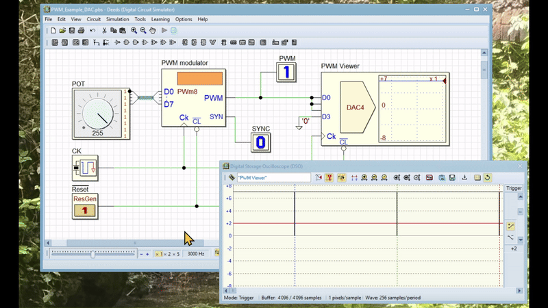
The animation demonstrates how the user can modify the duty cycle of the output signal by rotating the potentiometer. The full resolution version can be downloaded here.
 How the component works
The PWM generator's output has a period equal to 1/256th the frequency of the clock CK. The duration of the high part of the PWM signal's is equal to the number presented at the data inputs D7..D0. For instance, if the number is 255 ('11111111'), the duration will be 255/256 of the period; if the number is one ('00000001'), it will be 1/256 of the period. If the number is zero, the output remains low.
The PWM output goes to a high state on the clock edge that follows the cycle in which the counter value matches the input value D7..D0. Subsequently, the PWM output returns to a low state on the clock edge that follows the cycle where the counter value reaches zero.
The SYN synchronization output activates every 256 clock cycles, marking the end of pulse generation and the internal counter's countdown from 255 to 0. The system captures the D7..D0 number on the clock's rising edge at the end of the SYN pulse. This process allows the PWM output to adopt the new duty cycle without any unwanted transients.
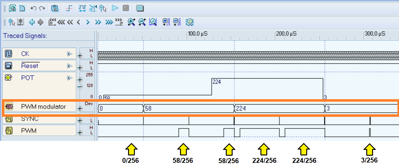
Timing Diagram simulation
The following image displays a Timing Diagram simulation of the PWM component. The PWM modulator track (highlighted in orange) reflects the values received from input D7..D0. The potenziometer input controls the duration of pulses (0/256, 58/256, 224/256, 3/256...) on the PWM output track.