 Digital to Analog Converter (DAC)
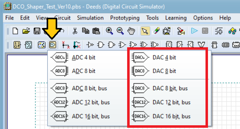
The Digital-to-Analog Converter (DAC) components are accessible in the component bar, as highlighted in the following figure. The user can choice between different bit-size (4, 8, 12 and 16 bits).
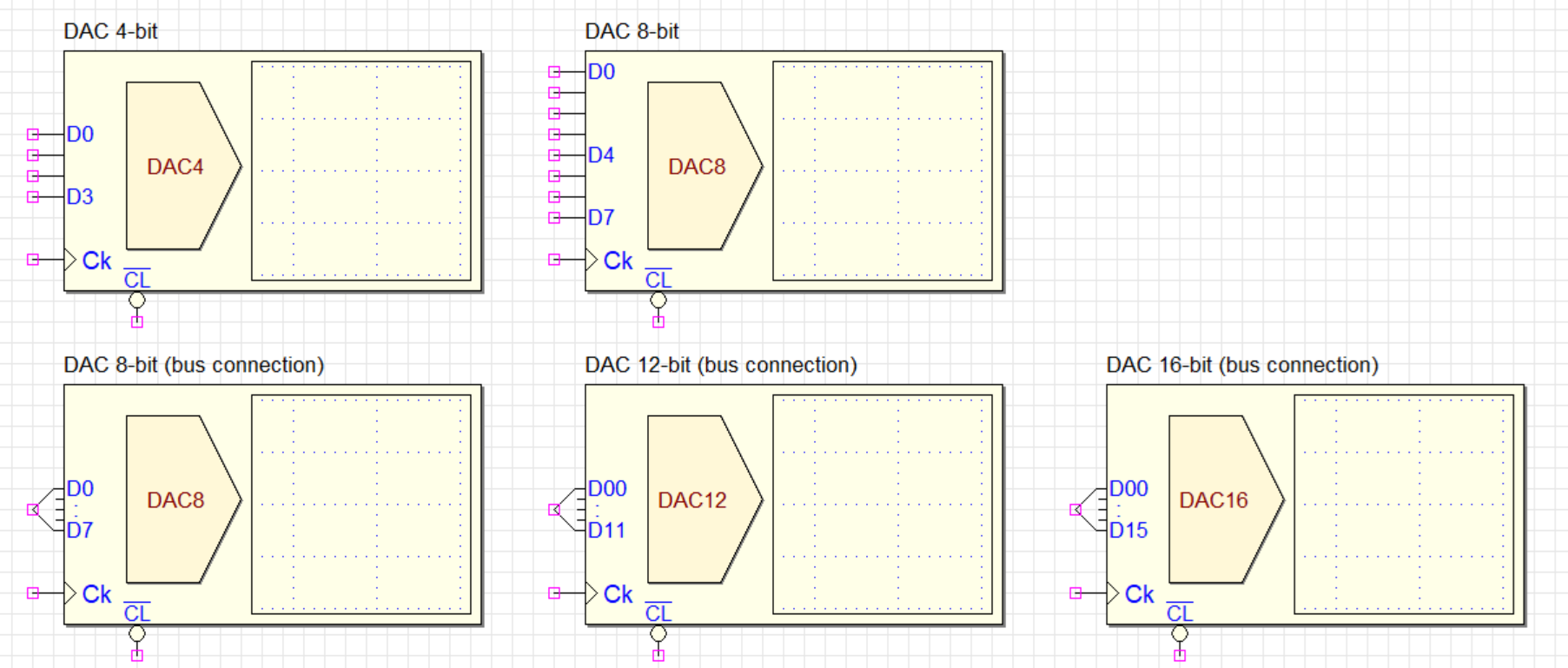
When placed in the schematic, the DACs are represented by symbols with a pentagon on the left, indicating the converter's functionality, and an empty square area on the right (see below).
The DACs are intended for displaying digital signals and accept signed numbers. During the simulation, the converted values are plotted 'by a pen' in the square area, forming a chart that logs the signal waveform (see the figure below).
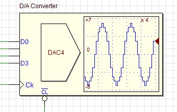
On the input side, the DAC acts as a parallel register, and a display device for the output data. On the positive edge of the clock (Ck), the data is loaded into the DAC register and then added to the display chart. When the clear input (!CL) is activated, the DAC register is cleared. Note that no analog output is physically generated.
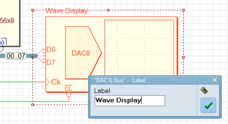
Double-clicking on the DAC component opens the Properties Dialog, where a specific label can be assigned to it (see the example below).
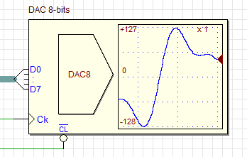
The circuit in the next figure shows an example of using an 8-bit DAC. The 8-bit counter cyclically generates all the 256 addresses of the ROM, which has been programmed with the 8-bit samples of an entire cycle of a sine wave. The resulting frequency will be F = Fck/256 (a click on the figure will open the file, automatically running the simulation).

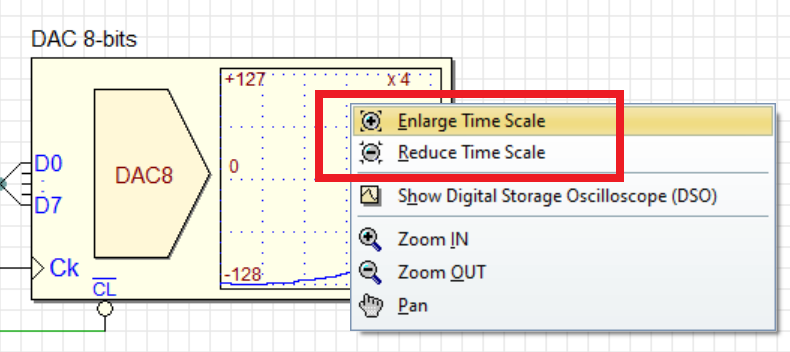
During simulation, the component's context menu (highlighted below) allows you to enlarge/reduce the display time scale (x 1, x 2... x 32).
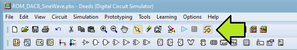
It is also possible to simulate the circuit in the Timing Simulation Window (click on the button pointed by the green arrow).
In this example, the Timing Diagram is setup to automatically load a test sequence. To start the simulation, click on the button highlighted by the white arrow in the screenshot below.
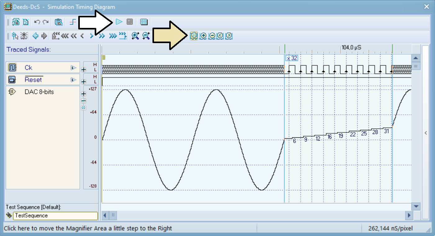
The figure also shows the possibility of enlarging an area of the diagram with the Magnifier, by clicking on the button highlighted by the yellow arrow.
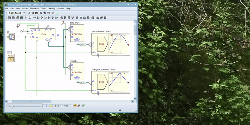
The following example shows the generation of two different waveforms (sine and triangle) having the same frequency. Again, clicking on the figure will open the file in Deeds-DcS, automatically running the simulation.

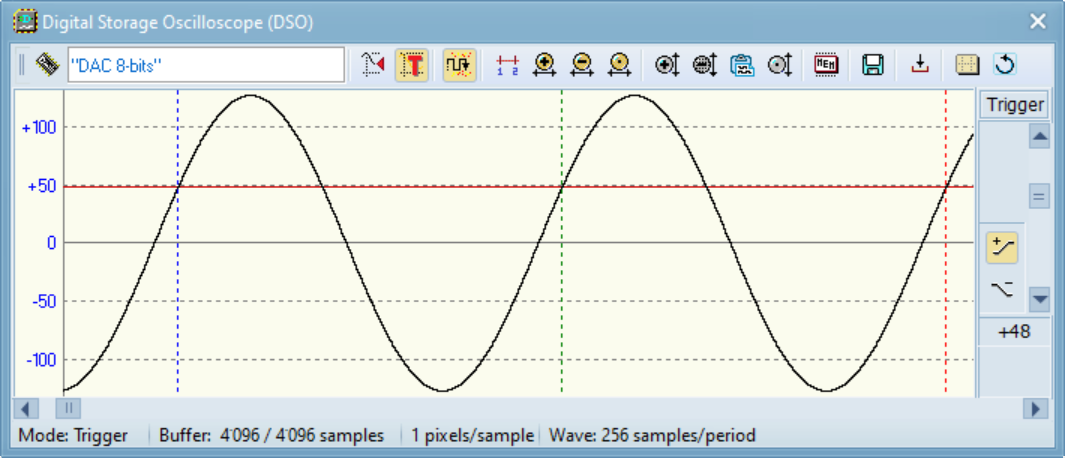
During both animated and timing simulation, you can open the Digital Storage Oscilloscope (DSO) by clicking on the component or using the context menu (see the figure below):
A short video demonstrates the network simulation and the waveforms displayed on two oscilloscopes.
You can download the video in full resolution here.
The description of the use of the DSO can be found here.