|
|
|||||||||||||||||
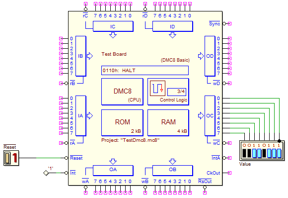
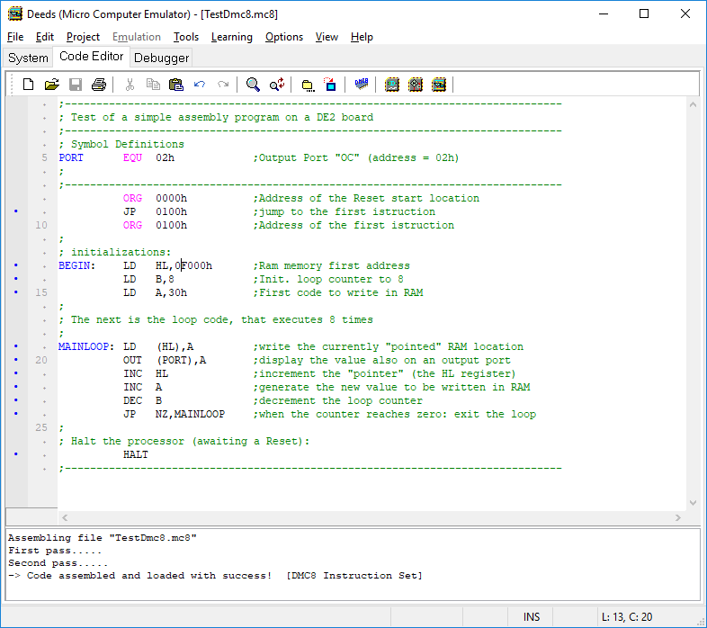
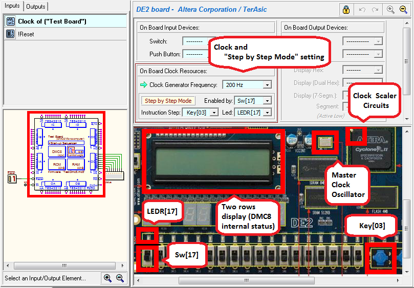
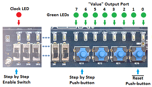
Before continuing, you should have read the pages: In this page we show the features offered by DEEDS for testing microcomputer systems (based on DMC8) on a FPGA board Terasic/Altera DE2 . We choose, as working example, a simple project. We have designed the following system (a click on the figure will open the schematic on the Deeds-DcS): A DMC8 microcomputer (in basic version) is connected to an 8-LEDs array through a parallel output port. The program that runs in the microcomputer is reported in the following figure (click on it to open the program in the Deeds-McE): As explained in the comments embedded in the assembly code, three registers are initialized at system reset. The system has been configured with 2 KB of ROM and 4 KBytes of RAM. HL is set to the address of the first available RAM location (F000h), B is set to the number of cycle repetitions that will be executed and, finally, A to the first character that will be written in memory, as explained in the following. The program mainloop writes, in 8 contiguous memory locations (starting from address F000h), the ASCII codes of the first decimal symbols (from '0' to '7': 30h, 31h, 32h, 33h, 34h, 35h, 36h, 37h), in the same order. For testing, at every loop cycle, the code is written not only in memory, but also onto the "PORT" output port. Last, the processor is halted (with a HALT instruction), waiting for a system reset. It is useful to test the network both in the animation To implement the system on the DE2 board, open in the Deeds-DcS the dialog window shown in the figure below, using the command “Test on FPGA”. In this example, all the associations between the schematic and the corresponding input/output devices on the DE2 are already set. The figure highlights the association of the microcomputer with the DE2 devices. The microcomputer clock frequency has been set very low (200 Hz), to allow a visual control of the output port (it has been associated to eight green LEDs on the board, see the figure below). The “Step by Step Mode” has been enabled, assigning to the switch Sw[17] the task to activate it at runtime. It has been selected a LED, LEDR[17], to visualize the clock pulses being sent to the microcomputer. Finally, the pushbutton Key[03] has been chosen to control the manual execution of the instruction (instead of selecting a pushbutton, the user could choose an continuous execution, from one instruction every ten seconds to five ones per second). If Sw[17] is at '0', the debug system is not active and the microcomputer works with the "normal" clock (200 Hz). If Sw[17] is turned on at '1', the system stops clock generation and the debugger waits for the user to press Key[03]. Each activation of the push-button executes one instruction (to do this, the debugger sends the number of clock edges that are necessary to execute the current instruction and to fetch (but not execute) the next one. A long pressure produces a continuous fetch and execution of instructions (approximately two per second). LEDR[17] will flash when an instruction is executed (a useful feature to highlight visually instruction steps). After an instruction is executed, the debugger reads the processor internal state and reports it on the alpha-numerical display of the board. The display has only two rows, so pages are continuously rotated to show all the processor internal registers contents. The following table shows some examples of display pages:
The following figure shows a comprehensive view of the associations and it can be seen as the “control panel” of our system: |
||||||||||||||||||


 and timing
  simulation modes of the Deeds-DcS. A proper test sequence is available in the timing simulation window. We recommend to avoid any change of the input/output terminations, already defined for exporting the project on the FPGA board.
