|
|
|||||||||
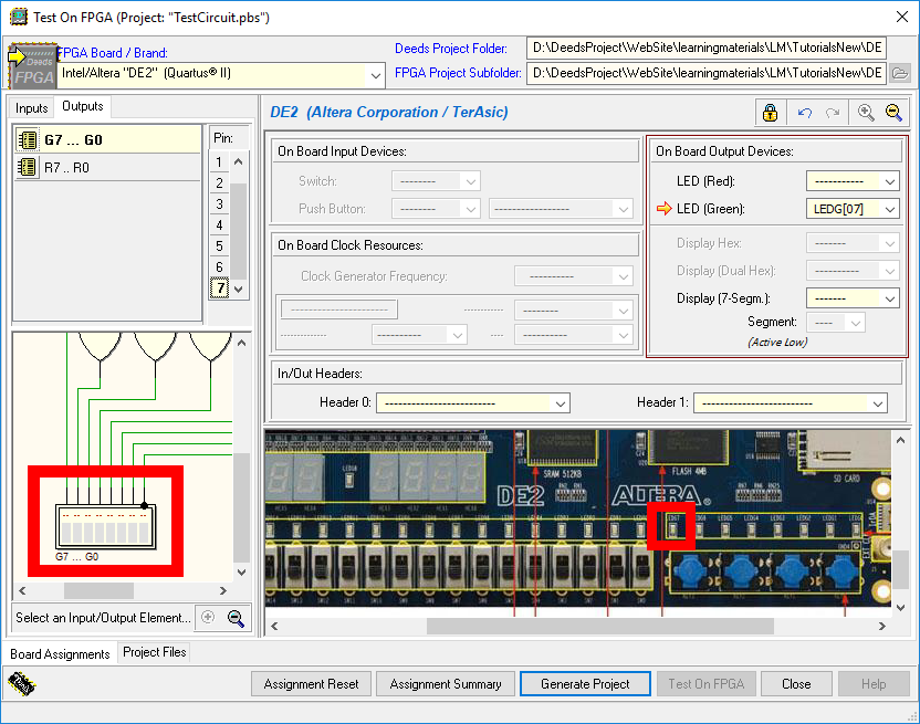
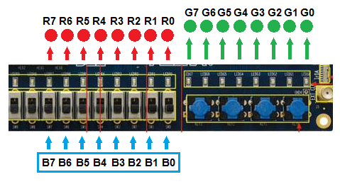
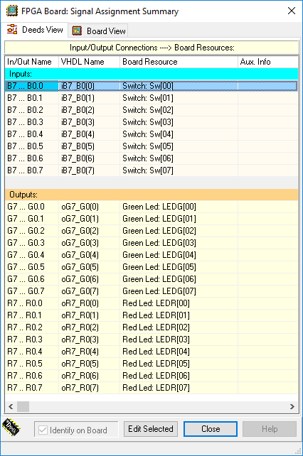
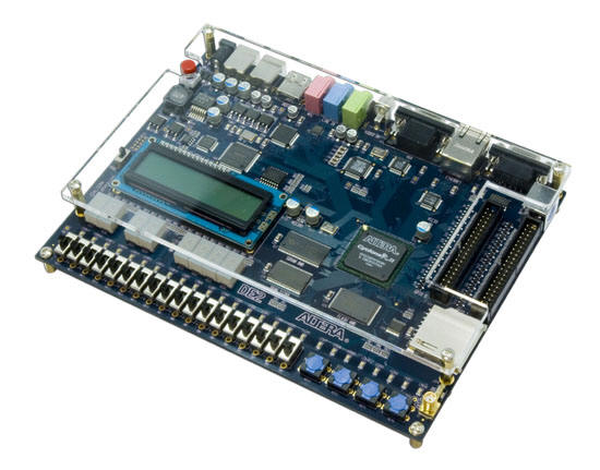
| In this page we examine the necessary steps to implement a DEEDS project on an Terasic/Altera DE2 FPGA board. The target is to implement a physical prototipe of the project and test its behaviour. Terasic/Altera DE2 board is conceived for the practical implementation of digital and mixed-signal circuits, even quite complex ones. It includes several I/O devices and interfaces, from simple ones (switches, pushbuttons, LEDs, seven segment displays) to complex devices (LCD matrix display, Ethernet network interface, USB 2.0, SD memory cards, analog audio I/O, analog video input, VGA video output and other). The core of DE2 is an FPGA ("Field Programmable Gate Array"), Intel/Altera Cyclone® II 2C35, composed by more than 30.000 Logic Elements (LE). DE2 may host simple introductory projects, like the one we are presenting here, and sophisticated ones that may include one or more microcomputers. . To focus on the method of the prototype implementation, let we use, as working example, a very simple circuit. We imagine that this circuit will be the result of our project activities, and that all the assigment specifications had been functionally verified, using interactive (and/or timing) simulation. The example circuit is a simple 8-bits code converter, from natural binary to Gray code (click on the following figure to open the schematic in the Deeds-DcS): The 8-bits code input is represented by the B7, B6, B5, B4, B3, B2, B1 and B0 lines. It is useful to verify the network behaviour in the Deeds-DcS, using both the animation At this point we begin the procedure for the physical implementation of the project in the DE2 FPGA board. The Deeds-DcS offers the command "Test on FPGA" (as highlighted in the following figure, available both in the "File" menu and in the command bar): The command "Test on FPGA" opens the dialog window shown below: In this window the user chooses firstly the FPGA board that intends to use (up left); then associates to each input and output of the Deeds-DcS schematic (highlighted in red on the bottom left of the window) one of the resources available on the board (highlighted in red on the bottom right of the window). As a reference, it is possible to download, as PDF, the DE2 board user manual. All the needed associations between Deeds-DcS schematic and the FPGA board input/outputs are already set in the given schematic: it is not necessary to modify them. For the convenience of the experimenter, the associations are highlighted also in the next figure, that can be considered as a "control panel", useful for testing the physical system: Eight of the available switches, Sw[07]..Sw[00] (nomenclature of the manufacturer), have been associated to the inputs B7.. B0; the eight red LEDs' LEDR[07]..LEDR[00] have been assigned to the outputs R7..R0; finally, the eight green LED's LEDV[07]..LEDV[00] are connected to the outputs G7..G0. Clicking on the button "Assignment summary", we can examine, as a table, all the assigned associations, both from the point of view of the schematic and from the point of view of the FPGA board:
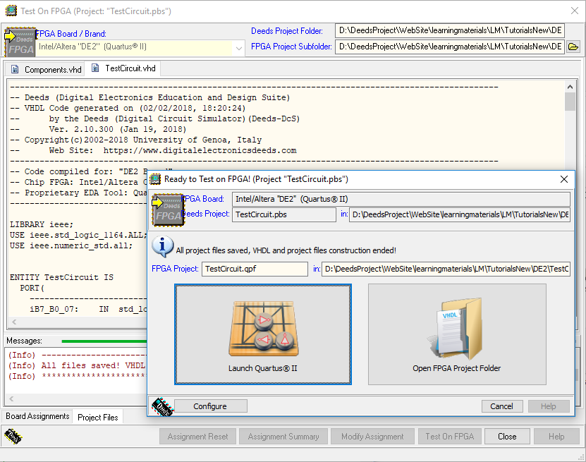
By clicking on "Generate Project", the Deeds-DcS will generate all the VHDL code and the project files necessary for the Quartus® II software, Intel/FPGA (ex Altera Corporation). VHDL is a HDL (Hardware Description Language) currently used for the design of digital systems, especially complex ones.
Quartus® II is available, free of charge, as web edition (ver. 13.0 sp1) and must have been previously installed on the PC that you are using. It is a powerful piece of software, with many development tools, for professional use. In our experiments we will use only the features that are necessary to transfer our project in the DE2. Once generated, the VHDL files will appear in the window, subdivided in different pages, as shown below. A dialog window (visible in the foreground) allows launching Quartus® II .
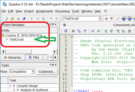
After the launch of Quartus® II, in its main window (up left), we can read the identifier of the FPGA Cyclone® II component used on the DE2 board, and the "top level entity" of the project:
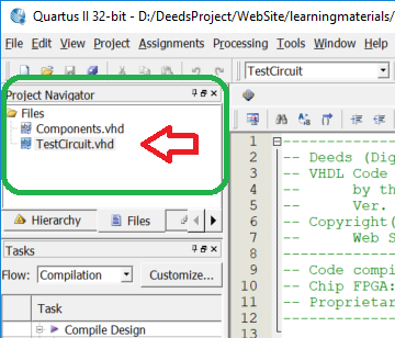
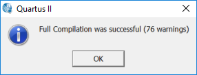
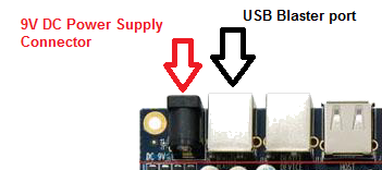
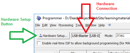
The Quartus® II Project Navigator shows that the project "TestCircuit.qpf" is opened. "TestCircuit.qpf" is one of the files that Deeds has generated (.qpf = "Quartus Project File"), it defines the "top level entity" of the project. Deeds has generated also the file "TestCircuit..qsf", that Quartus II uses to store all the relevant informations for the project synthesis, i.e. a list of the VHDL file to be compiled, and the Input/Output assignment to the board devices (switches, buttons, Leds, etc.). A click on the tab "Files" shows the VHDL files associated to the project. A double click allows the examination of their contents in the text editor. In this example, the file "TestCitcuit.vhd" is the structural description of the digital network, and matches the network schematic connections. The button "Start Compilation", in the command bar of Quartus® II, launches the compilation of the project: During compilation, the "Tasks" section of the Quartus® II main window updates the user on the progress of compilation. The window in the bottom shows the messages generated by the compiler. Last message should be similar to the following one: At this point it is necessary to transfer the compilation's result to the DE2 board, in order to configure the FPGA chip for the physical implementation of our project. The board needs power: its power supply should be connected to the proper connector ("DC 9V", see figure). The data transfer for the FPGA configuration takes place through the USB cable connecting the personal computer to the "USB Blaster" input of the board: Finally, the red button (top left of the board) powers up the DE2 and starts executes automatically a test program that flashes LEDs, shows the numbers from 0 to 9 on the seven segment displays and the message: "Welcome to the DE2 board" on the LCD matrix. A click on the icon "Programmer" begins the operations for FPGA configuration: A window for establishing communication with the hardware opens up. The figure shows the area we are interested to:
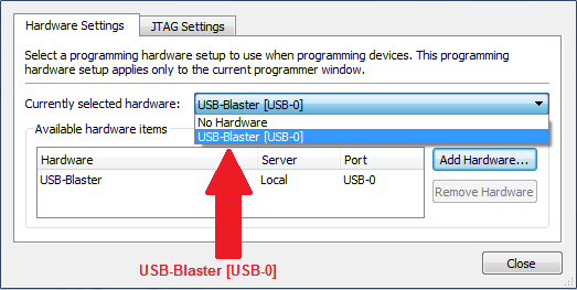
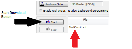
Choose "USB-Blaster" connection (red arrow in the figure). If the "No hardware", or other warning appear, it is necessary to power on the FPGA board, in the case it is off, and click on the button "Hardware Setup". The window will appear: Please select "USB-Blaster [USB-0]". We go back now to the programmer's window: A click on "Start", as shown by the black arrow, will transfer on the FPGA board the file "TestCircuit.sof", replacing the default test configuration. The blue LED "Load" will flash. Now the DE2 has become our system! Using the buttons shown in the previous figure and observing the status of the LEDs it is now possible to test the system. Before testing Deeds projects on FPGA, please read the following pages: | ||||||||||

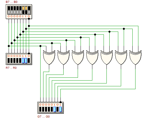
 and timing simulation
  . A test sequence is available in the Timing Diagram window, where a 16 numbers sequence is defined (from 0 to 15 dec.). We recommend to use the schematic supplied, without modifying the input and output terminations, since they contain the information needed for exporting the project on the FPGA board.
