|
|
||||||||||
| In this laboratory we'll work on a DMC8 assembly program that emulates an Asynchronous Serial Receiver. The receiver will expect data packets as the one described in the following figure:
The data packet is composed as follows:
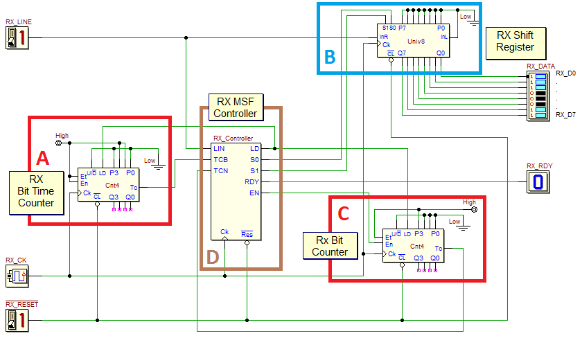
The next figure shows a FSM-based version of the receiver (click on the figure to open the schematic in the d-DcS editor): The system is composed of a bit time counter [A, highlighted in red], on the left hand side of the figure, a shift register [B, in blue, top-right], a bit counter [C, in red, on the right], and a controller [D, in brown, based on a finite state machine].
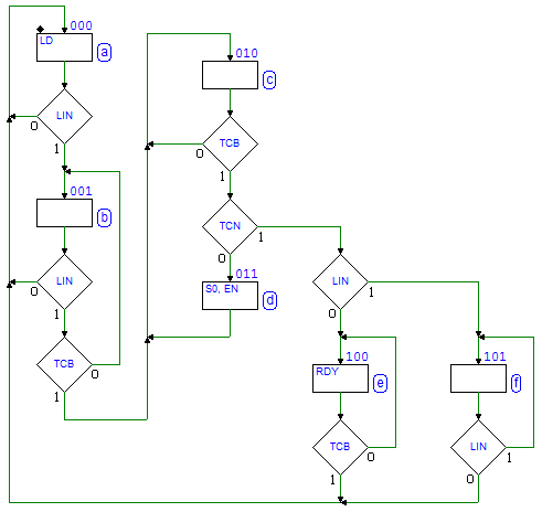
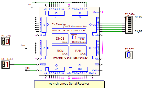
The controller clock frequency is 16 times the bit rate of the received packet. To catch the Start Bit, the controller samples its input LIN (alias RX_LINE) at every positive clock edge, in state (a). When LIN goes high, the controller continues to sample it, at the same rate, in state (b). If LIN is sampled always high, until the middle of the bit time is reached, the controller declares valid the Start Bit, and goes in state (c). On the contrary, if LIN returns to low, operations are restarted, looking again for a next valid start bit, in state (a). Note that the middle of the bit time is signalled by the TCB line, that is generated by the Bit Time Counter. This one is initialized, by means of the LD line, in state (a), to the starting value '0110'. As a result of this initialization, the first occurrence of TCB is generated on the middle of the bit time; the next occurrences, instead, will be generated every bit time (i.e. every 16 clock cycles, the counter cyclicity). The controller checks TCB also in state (c), to synchronize the operations of the RX Shift Register. When TCB goes high, the controller sets S0 = '1' and S1 = '0', in state (d), causing the RX_LINE data acquisition (on InR of the Univ8 component) and the right shift of all the other bits of the register. This couple of states (c,d) is repeated 8 times, i.e. until TCN is activated. TCN is generated by the RX Bit Counter when it reaches '0000', i.e. when the received data bits are over. Note that the RX Bit Counter is decremented, by means of EN, in state (d), each time a bit is acquired in the shift register. The next task of the algorithm relates to the Stop Bit validation. In state (c), when TCB is activated, but all the data bits have been received (TCN = '1'), instead of acquiring the Stop Bit in the shift register, the controller checks directly its value. If the Stop Bit is zero, the packet is assumed valid, and the RX_RDY signal is generated, in state (e), for the duration of a bit time. Otherwise, if the Stop Bit is high, the received data bits will be ignored (because the RX_RDY signal is not generated) and the algorithm will re-start from state (a). The loop state (f) is a simple attempt to recover the error state due to the wrong stop bit. In state (f) the controller waits for a low value on LIN, before to catch the next start bit (although this solution couldn't be the better one to handle a wrong stop bit reception). You can test the circuit using the d-DcS simulator, in Animation Mode The previous analysis of the circuit operations will help you to implement the same functionalities with a microcomputer system, based on the DMC8. The microcomputer-based serial receiver will look like the following schematic. Click on the figure to open the schematic into the d-DcS. In this network, the microcomputer is connected to the serial line RX_LINE using the bit 0 of the input port IA. We use the port OD to connect the RX_DATA output lines, and the port OC, on the bit 7, to generate the RX_RDY output. Note that no other component is used and that no RX_CK clock is connected to the microcomputer. All the time intervals needed will be calculated by the microcomputer, using delay routine techniques (the microcomputer clock frequency is 10 MHz). Click here to load a trace of a possible implementation of the assembly program. When finished to write and test the program in the d-McE, you'll load it in the ROM of the microcomputer and simulate the new circuit version in the d-DcS. Note that, to test the transmitter, the "RX_Sequence" input sequence is already available in the timing diagram. | |||||||||||


 Bit Time Counter [A]
 and in Timing Mode
  . A proper test sequence is available in the timing simulation window.