|
|
||||||||||
| In this laboratory you are guided to write a DMC8 assembly program that emulates an Asynchronous Serial Transmitter. It generates data packets as the one described in the following figure:
The data packet is composed as follows:
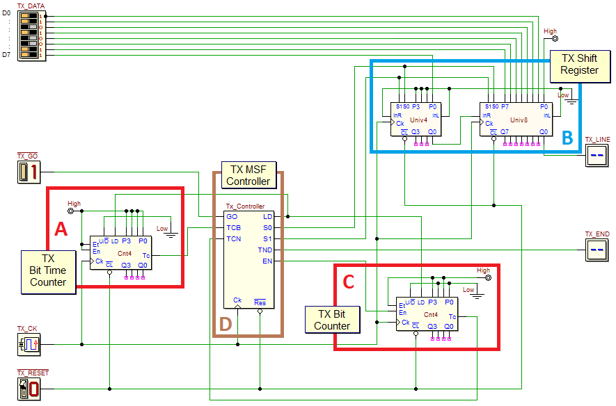
The next figure shows a FSM-based version of the transmitter (click on the figure to open the schematic in the d-DcS editor): The system is composed of a bit time counter [A, highlighted in red], on the left hand side of the figure, a shift register [B, in blue, top-right], a bit counter [C, in red, on the right], and a controller [D, in brown, based on a finite state machine].
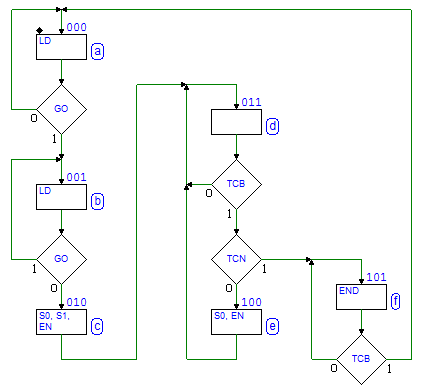
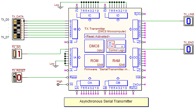
The !TX_GO command (GO for the FSM) starts the transmission: the first two states (a) and (b) are in charge of waiting for the pressure of the push-button ("low" when pressed) and also to activate LD, to preset all the counters. In the state (c), the activation of S0 and S1 loads the parallel data in the shift register, while EN causes the decrement of the number of bits to be transmitted. In the state (d), the controller waits for a TCB signal from the bit time counter: when it occurs (every 1,6 mS), the controller activates (e) the right shift of the data register (S1 = '0', S0 = '1') and decrement the number of bits to be transmitted (EN = '1'). When the number of bits to be transmitted becomes zero (TCN = '1'), the controller reaches state (f), where it generates the END output, to signal the transmission end. Finally, the controller returns to state (a). You can test the circuit using the d-DcS simulator, in Animation Mode The previous analysis of the circuit operations will help you to implement the same functionalities with a microcomputer system, based on the DMC8. The microcomputer-based serial transmitter will look like the following schematic. Click on the figure to open the schematic into the d-DcS. In this network, the TX_LINE is generated by the microcomputer on the bit 0 of the OD output port. Port IB is connected to the TX_DATA input lines, and port IA, on bit 0, reads the !TX_GO push-button. The OC output port generates the TX_END signal, on bit 0. Click here to load a trace of a possible implementation of the assembly program. When finished to write and test the program in the d-McE, you'll load it in the ROM of the microcomputer and simulate the new circuit version in the d-DcS. Note that, to test the transmitter, the "TxSequence" input sequence is already available in the timing diagram. | |||||||||||


 Bit Time Counter [A]
 and in Timing Mode
  . A proper test sequence ("TX_Sequence") is available in the timing simulation window.