|
|
||||||||||
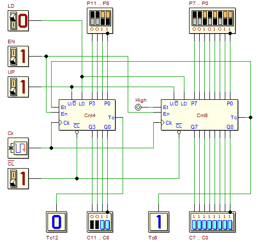
| In this lab we analyse a 12-bits binary counter, that use two d_DcS library components: Cnt4 and Cnt8. After verification with the simulation, we will implement a physical prototype on FPGA and test it. Click on the figure to open, in the d-DcS, the following test circuit: The Cnt4 component is a synchronous 4-bits binary counter, module 16, Up/Down, Presettable. The Cnt8 component is similar, but uses 8-bits, and it is module 256. In the schematic, C11..C0 are the 12 counter outputs (C11 = MSB, C0 = LSB). The clear input !CL is asynchronous: when it is active (='0') the outputs C11..C0 are forced to zero, with no regards for the other control and clock inputs. The load input LD is synchronous: when !CL is inactive and LD is active (='1'), the inputs P11..P0 are copied to the outputs C11..C0, on the rising edge of the clock input CK (when LD is active, the other inputs EN and UP are ignored). The enable input EN and the direction input UP are synchronous. They control the counting mode. When !CL and LD are inactive, if EN is inactive (='0'), counting is inhibited. Instead, if !CL and LD are inactive, and EN is active, at every rising edge of the clock CK, the C11..C0 value is incremented by one if the input UP is high, or decremented by one if the input UP is low. The terminal count output Tc12 is activated by the counter, for one clock cycle, when the outputs C11..C0 reach the maximum value ('1111.1111.1111' = 4095), if the count is forward. If the count is backwards, Tc12 is activated when the outputs C11..C0 reach the minimum value ('0000.0000.0000'). The circuit also generates the intermediate terminal count Tc8. The input Et of the counter Cnt8 is always active, so the functionality of Tc8 is always enabled, even when the count is disabled with EN = '0'. Tc8 is connected to the input Et of Cnt4: it enables the count of Cnt4, for one clock cycle, only when the low part of the count, on Cnt8, has reached the maximum (or minimum) value (depending on the count direction). You are requested to test the behaviour of the counter,
using the d-DcS timing simulation
At this point we begin the procedure for the physical implementation of the project in the FPGA board.
The general procedure is described in the introductory tutorials:
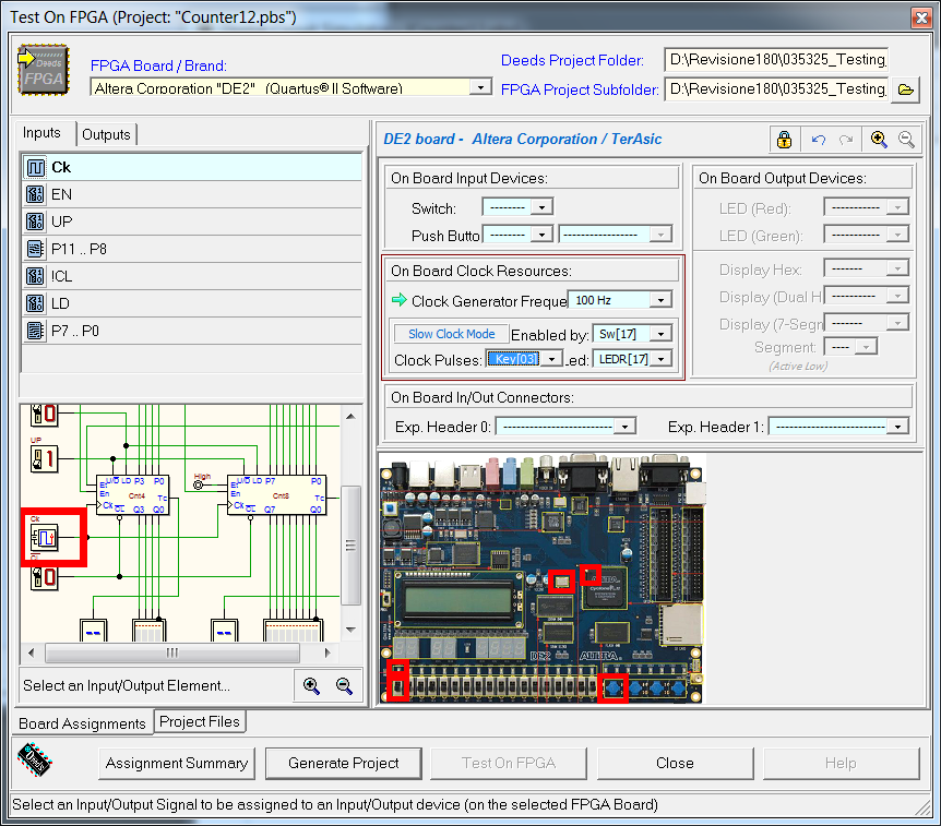
The command "Test on FPGA" opens the dialog window shown below: The clock CK is set to 100 Hz, a frequency rather low but adequate for the human interaction with the system. The "Slow Clock Mode" has also been set: as configured in the figure above, this mode is activable at run time using switch SW[17]. The "Slow Clock" is set to the manual mode, using the push-button Key[03], and it is displayed by the red LED LEDR[17]. According to this setting, if the switch is set to zero, the clock CK will work at the "normal" frequency of 100 Hz; if the switch is set to one, the clock will be generated one pulse at a time, when the user press the push-button Key[03]: in this mode, the network functionality can be tested with a simple visual observation. Note that the clock programmability feature is not a particularity of the FPGA board, but it is obtained by the design exportation process. This process adds a network to the project, based on counters, that "scales down" the on board 50 MHz clock to the desired low frequency. All needed associations between d-DcS schematic and the FPGA board input/outputs are already set in the given schematic: it is not necessary to modify them. For the convenience of the experimenter, the associations are highlighted also in the next figure, that can be considered as a "control panel", useful for testing the physical system: Using the switches and buttons shown above, and observing the status of the LEDs, it is now possible to test the system. | |||||||||||


 .
In the following figure we suggest a suitable input timing sequence for
the simulation (defined in the timing diagram window), although it can be useful to 'explore' other
interesting combinations of input signals sequences:


