|
|
||||||||||
In this laboratory you are asked to complete the design of an asynchronous serial communication system (see the figure below). After the simulation of the project, you'll realize a prototype on FPGA to verify the actual operations.
The system is composed of two identical units, A and B, interconnected between them, at a distance, through two serial communication lines. Each unit includes a transmitter (TX) and a receiver (RX). Each unit works with a nominal clock frequency of 10 MHz. The clock generators of the two units are physically different and separated: due to manufacturing tolerances, the actual frequencies of both will be a little different. Thus, the communication between the two units must be considered asynchronous. The two units communicate with each other by sending and receiving serial packet sequences (see figure below):
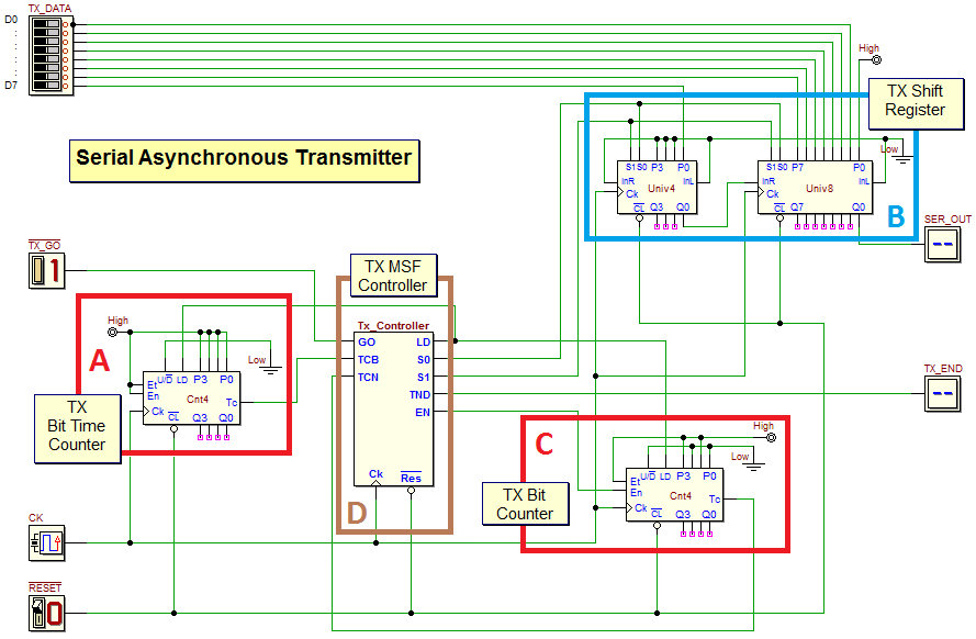
Each packet is composed of a START bit at '1', followed, in order, by the bits D0, D1, D2, D3, D4, D5, D6 and D7, and terminated by a STOP bit at '0'; the "bit time" is equal to 1.6 µS, corresponding to 625 Kb/s (10 MHz /16). Note that the clock is not transmitted to each other: the result is then an asynchronous serial transmission. The serial transmitter TX The following figure shows the schematic of the transmitter only, of which we will design the controller, after the analysis of the functionality of the other system elements. Task of the transmitter is to send on the SER_OUT line, when the user presses the !TX_GO button, a serial packet containing the data D7..D0 (at the TX_DATA input), according to the format and timing described above. At the end of the transmission, it activates the output TX_END for the duration of a bit time. In the figure we observe, highlighted by colored boxes: a bit time counter [A, in red], a shift register [B, in blue], a bit counter [C, in red], and the transmission controller [D, in brown], based on a finite state machine (FSM).
Serial transmission starts when data is loaded, since the loading operation sets the Start Bit on the line SER_OUT. The controller then obtains the transmission of the successive bits of the package, one after the other, by shifting the register to the right (setting S1 = '0' and S0 = '1'), for the duration of a clock cycle, at the end of each bit time.
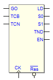
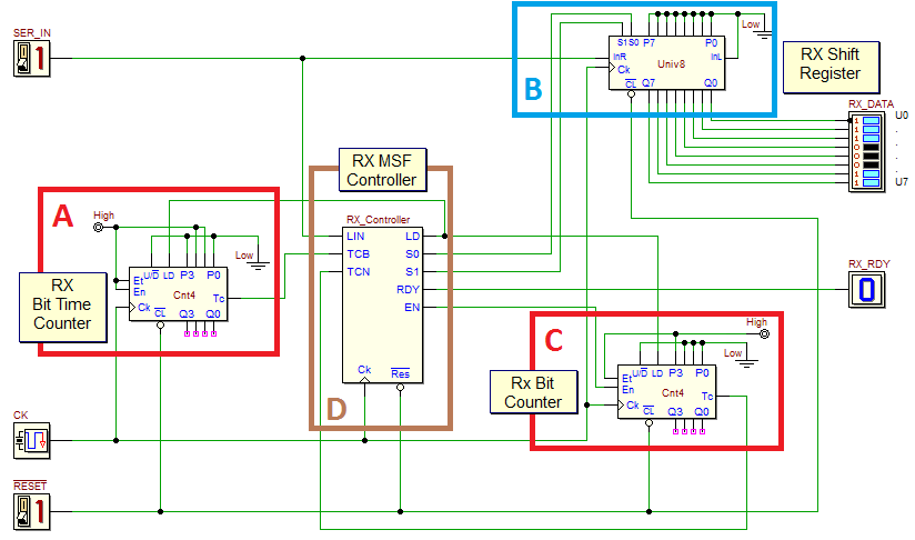
Design specifications of the transmission controller You can download here a ASM diagram, to be completed, of the transmission controller, where the state variables X, Y and Z have already been defined, as well as the outputs LD, S0, S1, END and EN, and the inputs GO, TCB and TCN (click on the picture to open the diagram to be completed in the d-FsM): The controller receives the command TX_GO (on the line GO): its falling edge initiates the transmission of data. In the diagram provided, the states (a) and (b) have the responsibility not only to wait for the falling edge, but also to initialize the transmission, activating the line LD. The controller also handles the transmission shift register: as described above, to start the transmission, it order the register to load the parallel data TX_DATA, along with the start and stop bits. The controller then enters a loop in which transmits the other bits by imposing a right-shift step to the register, on each activation of TCB. Finally, the controller activates the output TND, to signal the end of transmission. To ensure that the duration of the output TND will be equal to a bit time, you should wait for the last time the signal TCB, and then go back to waiting for the falling edge of GO. Using a d-FsM simulation, verify that the functionality of the designed FSM will match the specifications. Then, import the new component in the d-DcS, to complete the schematic available here. In the given schematic, some control outputs have been added, useful for a timing simulation (a suitable test sequence "TxSequence" is available in the timing diagram window). The serial receiver RX The figure below shows the block diagram of the receiver only, whose job is to decode packets arriving on the serial line SER_IN, taking into account the format and timing of the transmission. At the end of a packet decoding, the receiver produces in parallel, on the outputs U7..U0, the 8 bits that there were contained, and signal their availability, activating the output RX_RDY, for the duration of a bit time. Even in this case, we will design the controller only, after analyzing the functionality of the other elements. To do this, we observe in figure: a bit time counter [A, in red], a shift register[B, in blue], a counter of the number of bits [C, in red], and the receiver controller [D, in brown].
The operation of the RX bit time counter is almost identical to the one of the transmitter, but with a significant difference in its initialization. Even in this case, the counter generates a pulse every 16 clock cycles (1.6 µS, the bit time) on the output Tc. This line, renamed TCB at the controller input, is used to synchronize the acquisition of the data bits, one at a time, in the center of the time interval reserved to each one. Activating LD, the controller initializes the counter to the value '0110', and not to the maximum value, so that, starting the count from the start bit reception, the activation of the first Tc will occur in the middle of the bit time.
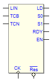
Design specifications of the receiver controller In summary, the controller, on idle, waits for the arrival of a packet on the serial line SER_IN. When the start bit is detected, its validity is verified and, thanks to this, all the operations of the shift register are synchronized, in order to correctly capture the next packet bits, and finally, to perform the verification of the stop bit (in the following these operations will be examined in more detail). As in the case of the transmitter, we can contain the algorithm of the controller in a reasonable number of states, as timings and counts are delegated to external devices. Here is available a ASM diagram of the controller, to be completed. In the file, the state variables X, Y and Z have already been defined, the outputs LD, S0, S1, RDY and EN, the inputs LIN, TCB and TCN and, finally, the states (a) and (b ) are already set (click on the figure will open the file in the d-FsM): Looking at the ASM diagram, in the wait state (a) the controller checks the serial line (at the input LIN), awaiting the start bit. In state (a), the activation of LD initializes the counters of the bit time and the number of bits: coming out from this state, the counters will then be free to count, starting from the initialization value. On the occurrence of the start bit, we switch in the state (b), awaiting the middle of the bit time (i.e. awaiting TCB activation). If, in the meantime, LIN returns low, the start bit format is considered invalid, and then we return to the initial state, awaiting a new start bit. Let us remember that, as said before, the bit time counter has been initialized so that it activates TCB, the first time, in the middle of the bit time: while we are in the state (b), the bit time counter is decreasing its value. Upon arrival of TCB, we declare valid the start bit, and continue beyond. Awaiting TCB in state (b), also, allows us to synchronize, with respect to the start bit, the acquisition of successive data bits. In fact, after the first activation of TCB, which occurred at the middle of the start bit, the bit time counter will continue to activate TCB cyclically every 16 clock positive edges, and thus always at the middle of the time of all subsequent bits. The acquisition of the 8 data bits is handled by a cycle of states in which the controller:
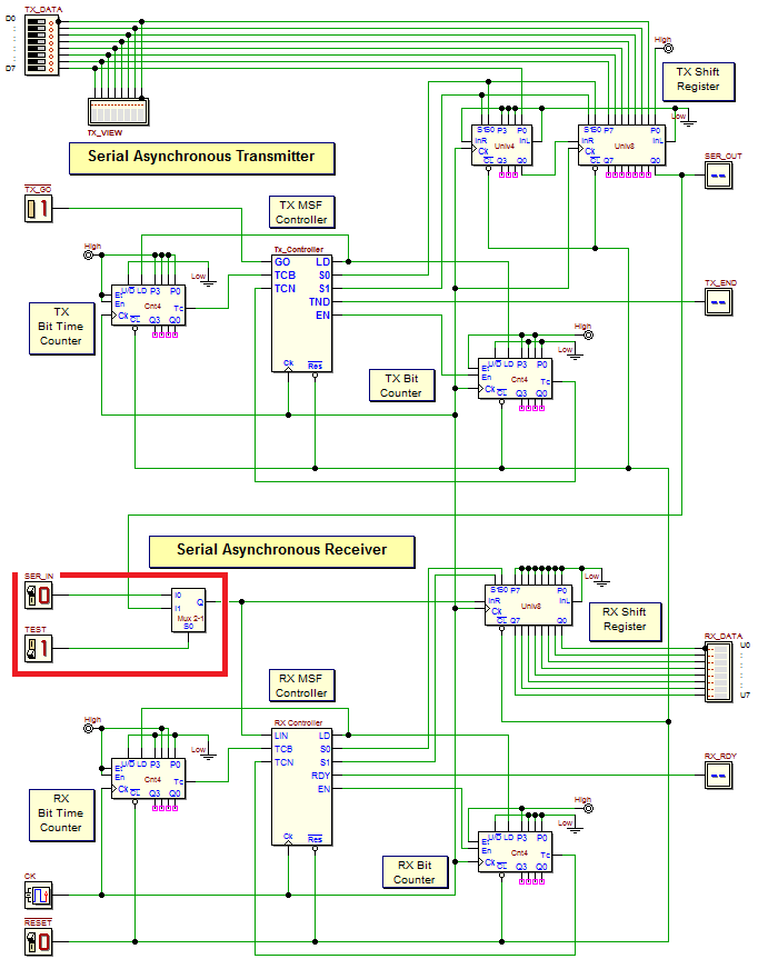
If TCB and TCN are both active, there are no more data bits to be received, and that's when the stop bit is available on LIN. It is not necessary to memorize this bit, but only to verify its value. If the stop bit is properly at '0', we just have to activate RDY for the duration of a bit time (awaiting TCB again) and then back again awaiting a new packet in state (a). However, if the stop bit value is wrong, we wait, without generating RDY, that the line LIN goes back to '0', than we return in the state (a). The functionality of the FSM can be verified, preliminarly, using the d-FsM simulator; then, the component obtained must be imported into the d-DcS, in the schematic, to be completed, available here. Again, a few control outputs have been added to the schematic, to make your timing simulation more readable (you can use the test sequence "RxSequence", defined in the timing diagram window). The complete unit (TX + RX) The following figure shows the schematic of the complete unit (transmitter and receiver):
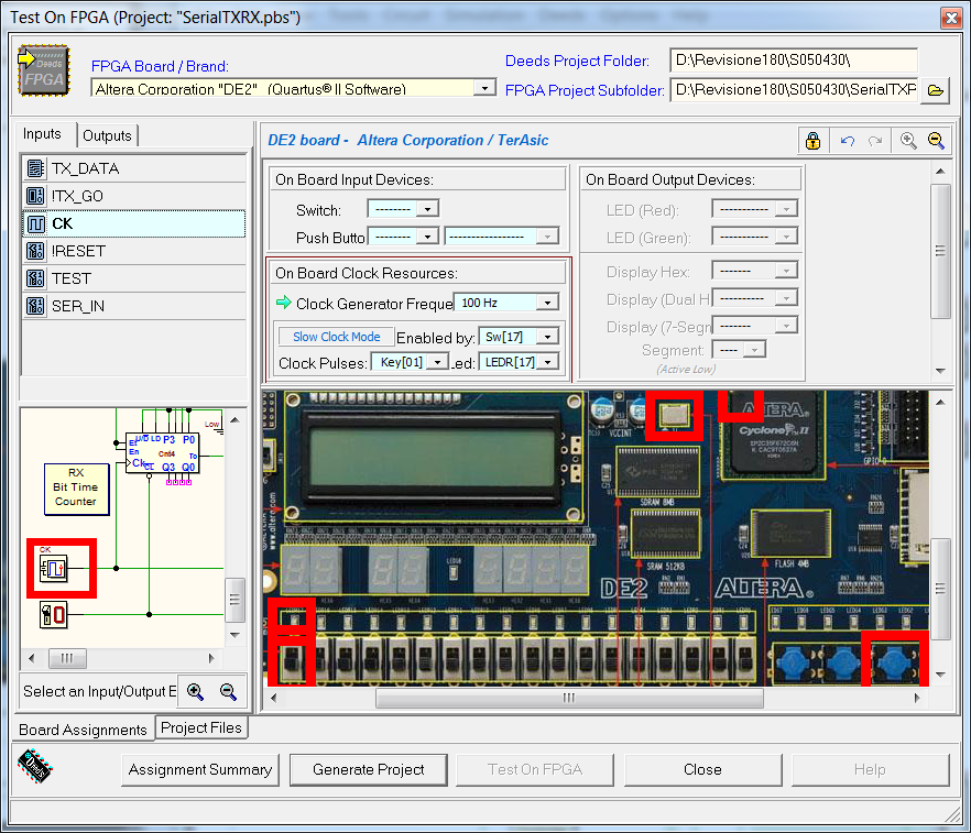
The transmitter and receiver are exactly those defined above. The clock CK and the !RESET have been unified, and are visible at the bottom of the schematic. A multiplexer "2-1" was added: in the diagram, it is highlighted with a red frame. The new TEST input, when activated, allows us to connect the receiver directly to the transmitter, to allow stand-alone testing, without the need to link two different systems. In this way, in simulation we are able to send a packet and receive it directly in the same system. To simulate the entire system of serial transmission and reception, we provide here a schematic, to be completed with the two FSM previously designed. The schematic, as in the previous cases, has been enriched with some control outputs, to make more complete the timing simulation (in the diagram window time is available the test sequence "TestSequence"). The added outputs will help also the experimentation of the system on the FPGA board. We recommend to use this schematic without delete or modify the input and output terminations because they have been set for the export of the project on the FPGA board. After the simulation of the entire system, let's move to its physical implementation on the FPGA board. The general procedure is described in the introductory tutorials: The "Test on FPGA" command (of the d-DcS) will open the dialog window visible in the next figure:
The associations between the d-DcS schematic and the FPGA board (inputs and outputs devices), have been already defined, so you do not need to change them. The clock CK is set to 100 Hz (rather than 10 MHz), to allow visual examination of the behavior of the system. The "Slow Clock Mode", set as shown in the figure above, will be activated at run time by the switch SW[17], and it is defined to work in manual mode (controlled by the push-button Key[01] and displayed by the red LED LEDR[17]). According to this setting, if the switch is zero, the clock CK will work normally at 100 Hz, but if the switch is at one, the clock will be generated a pulse at a time, at each activation of the push-button. To optimize the testing of the serial communication system on the FPGA board, associations are highlighted in a summarized way in the figure below (the "control panel" of our system):
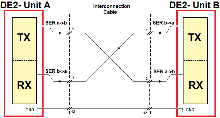
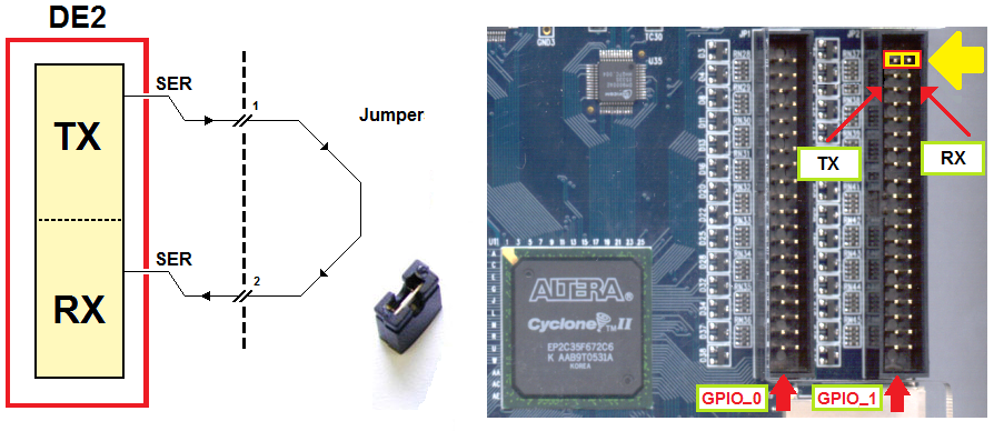
We can test the system stand-alone by activating the test mode (switch TEST upward), or by using two separate boards, interconnected by means of an appropriate cable, to exchange data in both directions: We make the connection using one of the two 40-pin connectors available on each FPGA board. As seen in the figure above, we use a cross-connection between the transmitter and the receiver, in both directions, for a total of 3 wires (including the ground reference GND). Here the pattern of the connection schematic, which refers to the expansion connector "GPIO_1" present on the board. Even without activate the TEST switch, we can perform preliminary tests with a single board, using a simple jumper inserted into the connector, as shown in the following figure (yellow arrow), in order to connect with the transmitter and receiver:
Be extremely careful in placing and removing the jumper, to avoid mechanical damage to the connector pins. To avoid possible damage to the FPGA chip, whose pins are directly connected to the connector, it is necessary to carry out this operation when power is off. | |||||||||||


 Bit Time Counter [A]