| ||
| Design of a serial line receiver |
|
|
| v2.41 |
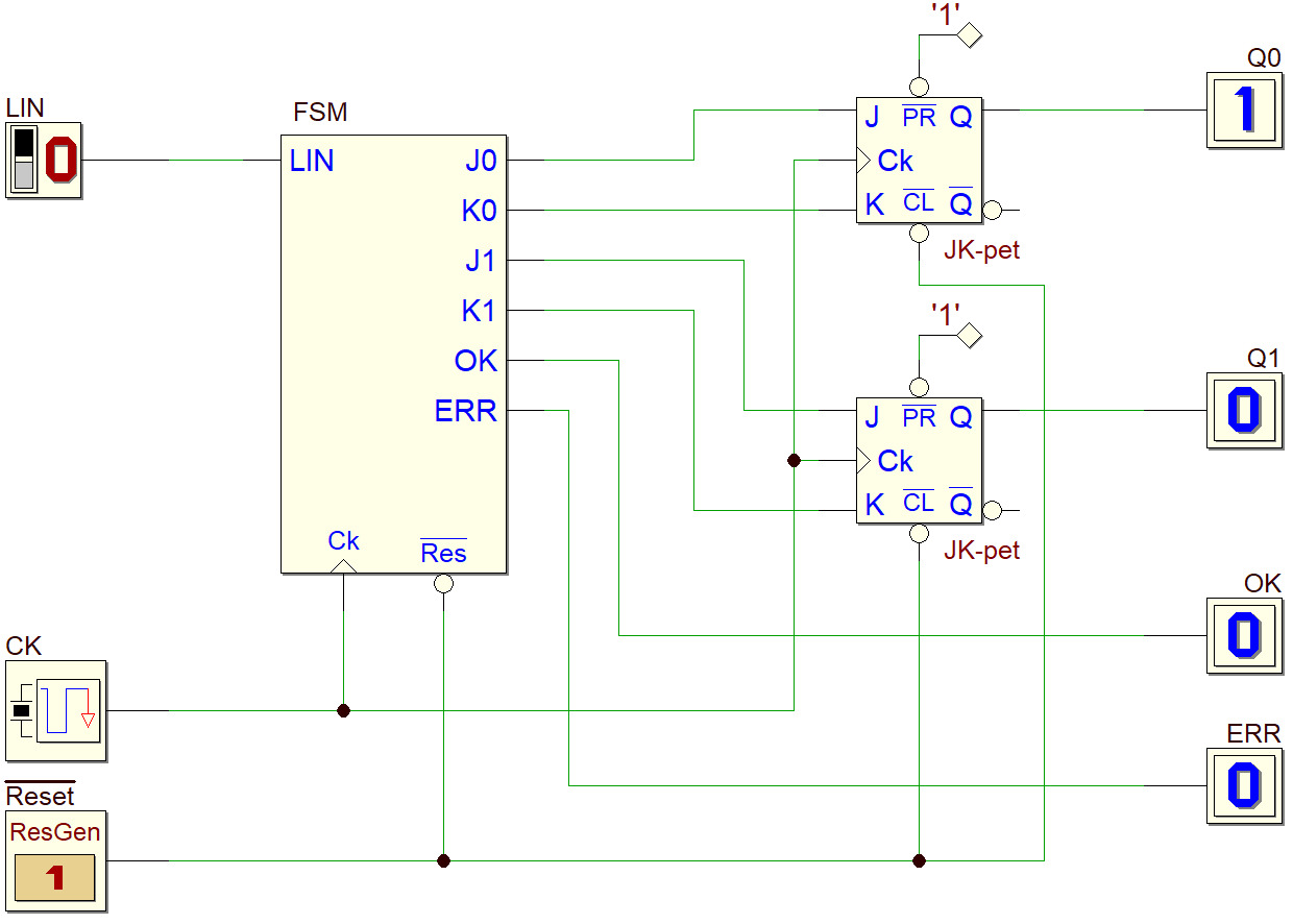
The following device is a 2-bit serial line receiver. The Finite State Machine (FSM) receives, through the input line LIN, a synchronous bit stream consisting of 4-bit packets. The FSM generates the two outputs OK and ERR and controls two JK-pet flip-flops through J0, K0, J1 and K1 (click on the figure to open the schematic to be completed in the Deeds-DcS editor).
LIN is at value '0' when no transmission occurs (two subsequent packets are spaced in time, between them, at least three clock cycles).
The Start Bit of each packet is always at '1' and the Stop Bit should be always '0'. The second and third bits carry the information that must be transferred on Q0 and Q1, respectively, by properly controlling the two flip-flops. The values transferred to Q0 and Q1 must be maintained until a new packet has been received.
If the packet is received correctly (i.e. the Stop Bit = '0') the FSM sets the output OK, otherwise it sets the output ERR. The values of OK and ERR are maintained until a new packet is detected on LIN.
The !Reset line, when activated at '0', forces the FSM to its initial state.
You are requested to design the FSM using the Deeds-FsM simulator (here the FSM file to be completed).
Then, simulate the behavior of the entire system using the Deeds-DcS simulator, with the FSM imported as a component.
We suggest, in the following figure, a test time sequence for the LIN input (it is already available in the Timing Diagram Window of the Deeds-DcS simulator):

Next, synthesize the FSM and re-draw the schematic substuiting the FSM component with the actual circuit obtained by synthesis. Verify the behavior of the entire new system using the Deeds-DCS timing simulator (please, apply the same time sequence used before).
Please, report a few comments about the differences between the timing results (if any).


