|
|
||||||||||
|
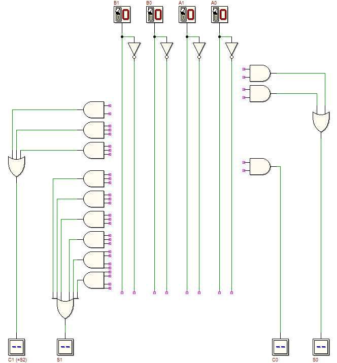
Load the following circuit in the d-DcS, with a click on the figure. This combinational circuit is an adder for two-bit numbers. The circuit is composed by a half-adder (the AND and the XOR on the right) and a full-adder (the six gates on the left). Note that the schematic does not represent a two-levels network. Start the functional simulation Now let us synthesize the above circuit as a two-level AND-OR network, building a fast adder for two-bit numbers. “Fast” refers to the fact that the number of levels of the resulting circuit will be only two, and the propagation time from input to output will result lower (this would be more in evidence if we'll compare adders for large-word numbers). Compile a K-maps for each of the outputs and write their expressions of the minimized synthesis. Draw the schematic of the resulting network. Click on the next figure to open in the d-DcS the schematic to be completed: Verify the circuit behaviour
through a functional simulation | |||||||||||


 and compile the truth table of the circuit. Verify the circuit behaviour also
through a timing simulation
  (a suitable test sequence is available in the Timing Diagram window).