Testing a Serial Communication System (4 bits) on FPGA
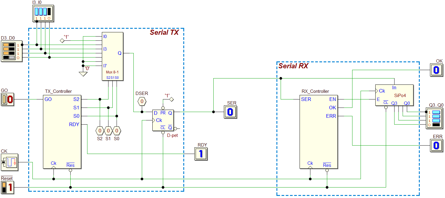
In this example, we start from the previous project (Synchronous Serial Communication System), to implement it on a FPGA board. For the operation details and the simulation of the system, refer to that project. Here is the schematic diagram of the network (a click on the figure will open the circuit in the Deeds-DcS):
We configure for the testing three different FPGA boards (the DE2, the DE0-CV and the DE10-Lite from Intel/Altera). If you click on the previous schematic, you open a file not yet configured for testing, but useful for practicing. However, if you prefer to skip this task, you can download here a file already configured for all the boards, and go directly to the final part of this example.
Let us guide you in configuring the file for FPGA testing. All the operations are described in the tutorials available on this site, but we recall anyway here a few examples of the procedure.
Open the “Test on FPGA” window, using the following command:

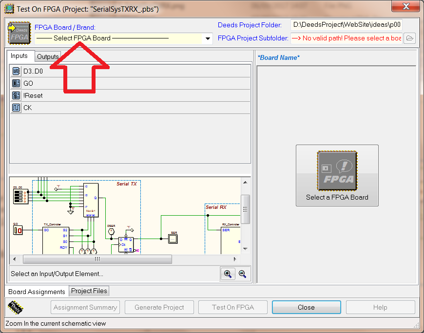
The first thing to do in the window is to select the FPGA board model that you want to use:
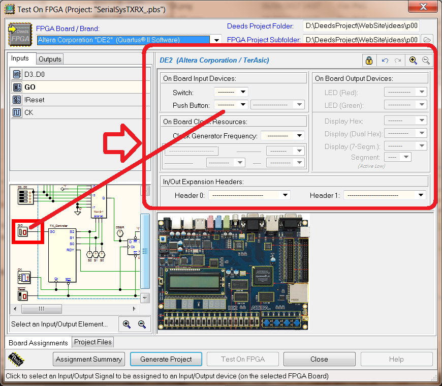
After this choice (in this example the DE2 board), you need to select, one by one, the components that you want to associate to the board resources (by clicking on the schematic below, or on the Input or Output elements list, above).
For instance, click the GO push-button visible on the schematic, or select it. As you see in the next figure, the GO component is selected in the Input list and, on the right hand side of the window, all the compatible resources on the board are available to be chosen: Switches, Push-buttons, etc.:
Now, we click the Push-button list box, that allows to select one among the four available on the bottom-right side of the board:
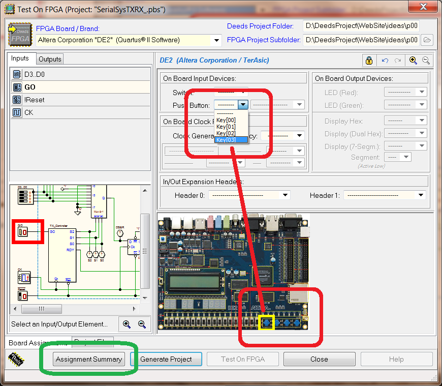
We select the Key[03], as highlighted in red in the figure above. This operation should be repeated for each Input or Output component in the schematic. When finished, you can verify all the associations using the Assignment Summary button (highlighted in green in the previous figure):
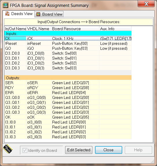
Now it’s possible to generate the VHDL and the project files necessary to compile the circuit on a FPGA, simply by clicking on the Generate Project button:

Deeds generates them, shows the VHDL files and prompts you to launch the specific CAD system (Quartus II, from Intel/Altera ):
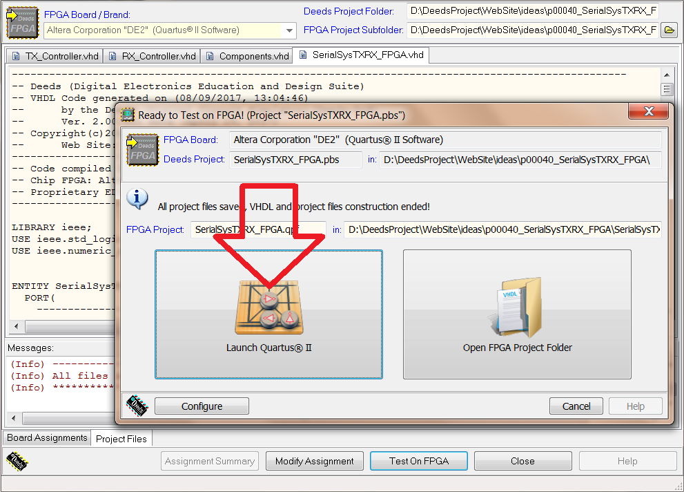
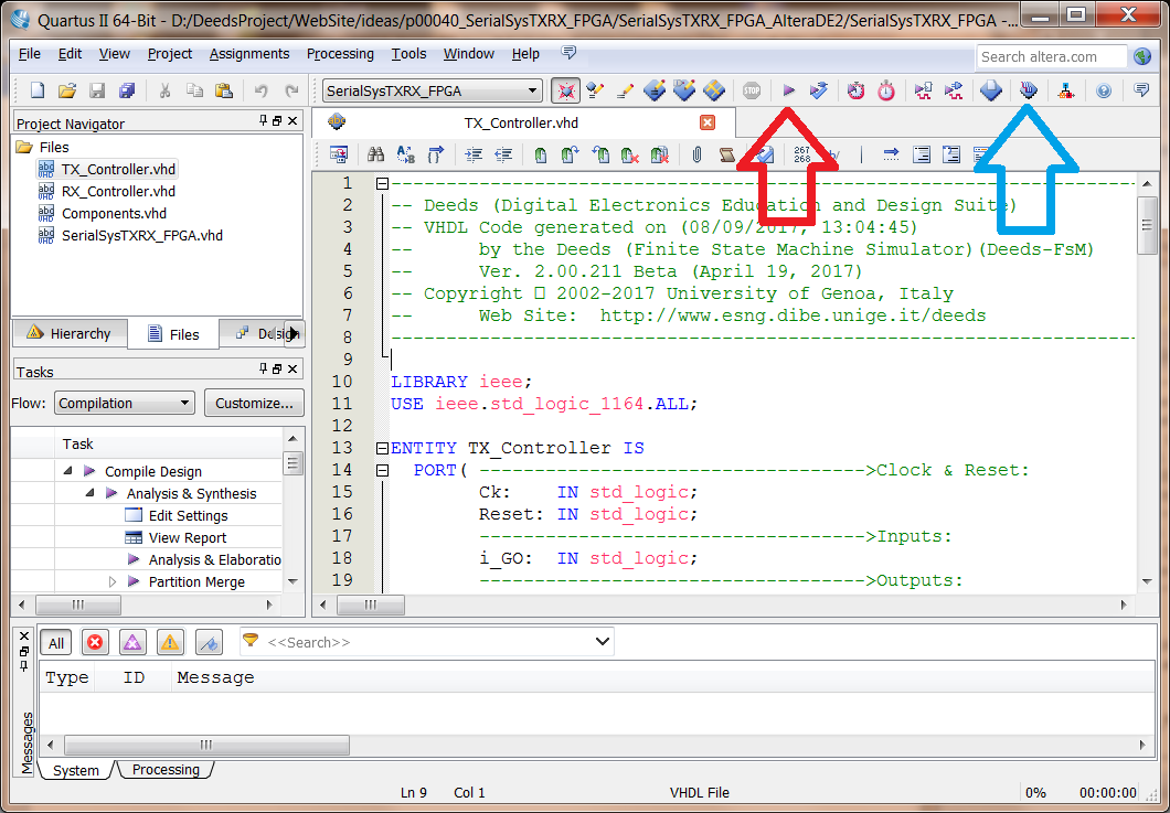
Please read the tutorials to see all the operation to be done to install and use Quartus II. Consider that you do not have to be familiar with Quartus II, except for two commands, highlighted in the next figure. They are necessary to compile the project (red arrow) and then to launch the FPGA programmer (blue arrow):
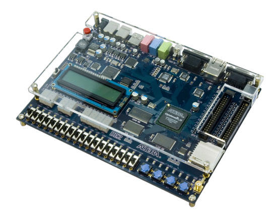
Finally, we have the circuit loaded, and operating, on the FPGA board:
To test the circuit, interacting with the board elements, it is useful to consider the next figure, that summarizes the Input-Output associations:

