Synchronous Serial Receiver (4 bits)
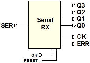
Let’s design a 4-bits synchronous serial receiver. The unit will receive serial sequences on SER, and generate the outputs Q0, Q1, Q2, Q3, OK and ERR, as shown in the next figure:
The format of the serial packet is:

- The bit sequence is synchronous with the clock CK;
- The bit time duration is equal to one clock cycle;
- Each sequence begins with a Start Bit (high);
- Four data bits follow (D0, D1, D2 and then D3);
- The bit packet ends with a Stop Bit (low).
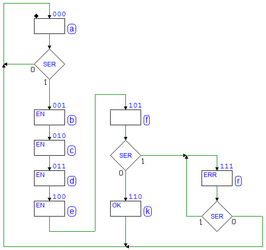
The receiver will copy the D0, D1, D2, and D3 values of a sequence on the outputs Q0, Q1, Q2 and Q3. The stop bit is correctly received if equal to 0: in this case the system will activate the OK output for the duration of a clock cycle. Instead, if the stop bit is equal to 1, the receiver activates the ERR output, until SER will return to 0. Then the receiver will return to wait for another packet.
Solution
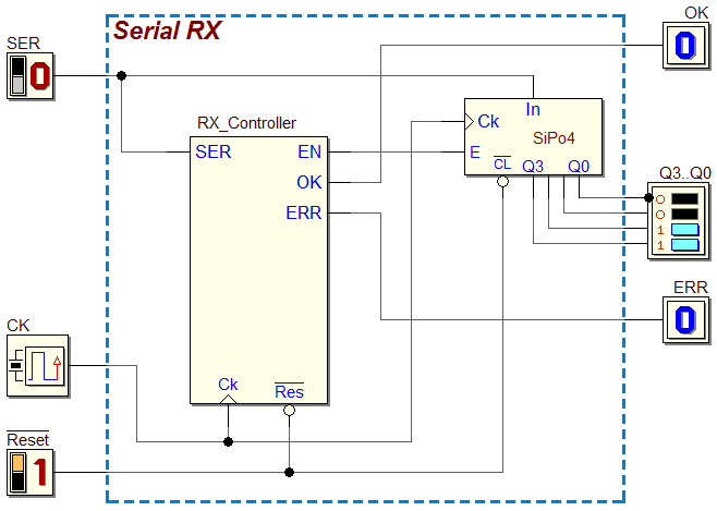
We use a Controller + Datapath structure; a shift register (we use the SiPo4 component , from the Deeds library) has the task of parallelizing and storing the data.
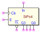
This 4-bits shift register receives serial data on the In input, and the output data is available in parallel on Q3..Q0. On the rising edge of the clock, if the enable input E is active (= 1), data shift by a position in the direction: In → Q3 → Q2 → Q1 → Q0. Otherwise, if E = 0, the outputs remain unchanged. The reset input !CL is asynchronous and active-low. When !CL = 0, outputs Q3..Q0 are cleared.
We connect the In input directly to SER. The shift register receives the data, bit after bit, converting it in parallel. The controller must synchronize the shift operations, enabling the register when needed by activating the EN line (a click on the figure will open the circuit in the Deeds-DcS):
The controller waits for the start bit; then enables data shifting in the register, until the stop bit time arrives. At that moment, the controller evaluates the stop bit value, activating OK or ERR, according to the specifications.
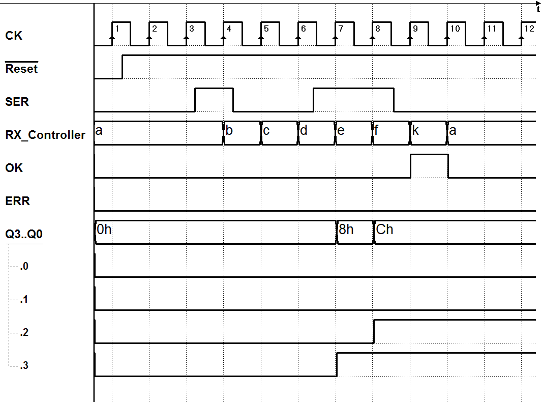
With the timing simulation we can verify if the system behaves correctly. As you see in the next figure, a test sequence (Start Bit=1, D0=0, D1=0, D2=1, D3=1, Stop Bit=0) has been set. OK is correctly generated after receiving the stop bit (on the clock edge 9), validating the Q3..Q0 outputs.
