Potentiometer-style Input Components
The rotary 'Potentiometer' components generate 8-bit input easily and interactively.
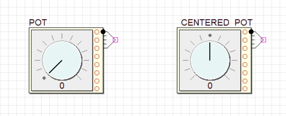
The only difference between the two types is the position of the 'Zero'. The left one generates numbers 0 to 255, while the other produces two's complement coded signed numbers, ranging from -128 to +127. Despite this difference, their behavior remains identical.
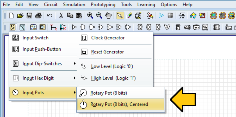
As shown in the following figure, you can now find the new Potentiometer components under the Input Components menu.
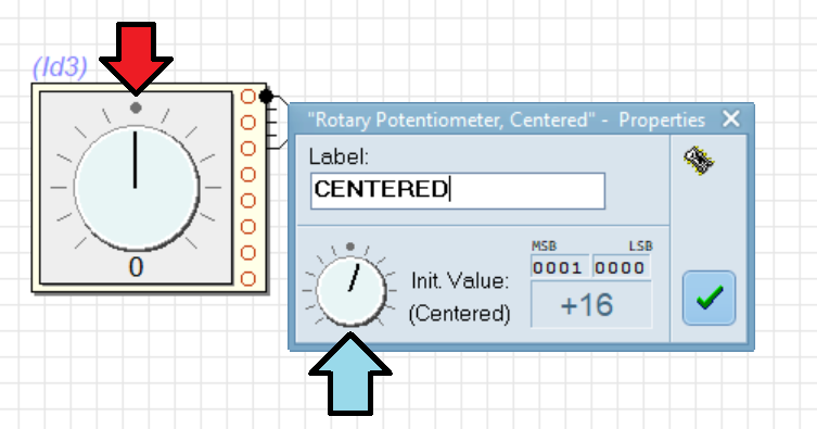
The Properties Dialog will appear when the component is inserted into the circuit. This dialog allows you to assign a label and set the initial value that the component will generate at the start of the Animated Simulation. Note that the zero position of the knob is marked with a dot on its leftmost, anti-clockwise position.
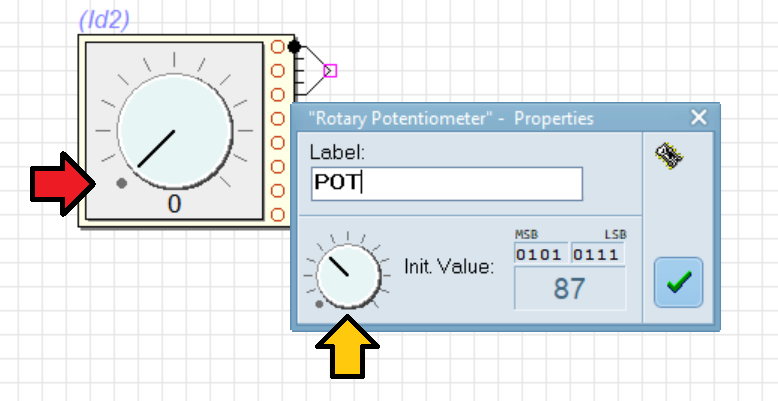
The knob of the potentiometer is adjusted by clicking, holding, and dragging the mouse toward the desired position. The mouse can be moved away from the knob while holding the mouse button to make fine adjustments. The new position is set when the mouse button is released. The value, in both binary and decimal, is displayed in the dialog box. A full clockwise rotation to approximately 270 degrees results in a value of 255 ('11111111').
The following image depicts the insertion of a zero-centered potentiometer type component. When this knob is fully rotated clockwise, the value is set to 127 ('01111111'). Conversely, rotating the knob fully counterclockwise will set the value to -128 ('10000000').
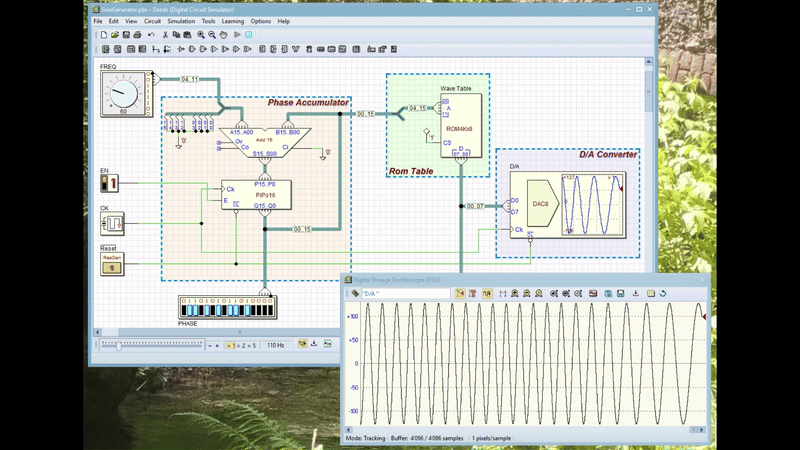
The included schematic demonstrates how the frequency of a sine wave, generated by direct synthesis, can be modified by utilizing a potentiometer. To interact with this example in Deeds-DcS, click on the circuit image.

An 8-bit DAC displays the samples of a sine wave that are read from a 4Kx8 ROM memory by the generator. The upper 12 bits of a 16-bit register, whose value is continuously increased by an adder using a parameter set by the potentiometer, are used to address the table in the ROM. The generated frequency (Fg) is equivalent to Fck * K / 4096, where Fck represents the clock frequency and K represents the output value of the potentiometer component (0..255). By adjusting the knob's angular position, the frequency of the output sine wave can be changed interactively.
The animation in the video below shows a simulation of the circuit. The frequency of the output sine wave is adjusted by dragging the angular position of the potentiometer with the mouse. The full resolution version can be downloaded here.
 The potentiometer in the timing diagram window
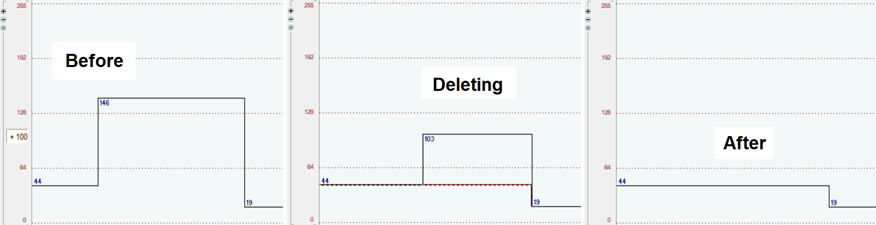
The value sequence of the potentiometer input track can be defined in the Timing Diagram Window, as shown highlighted in red in the following screenshot.
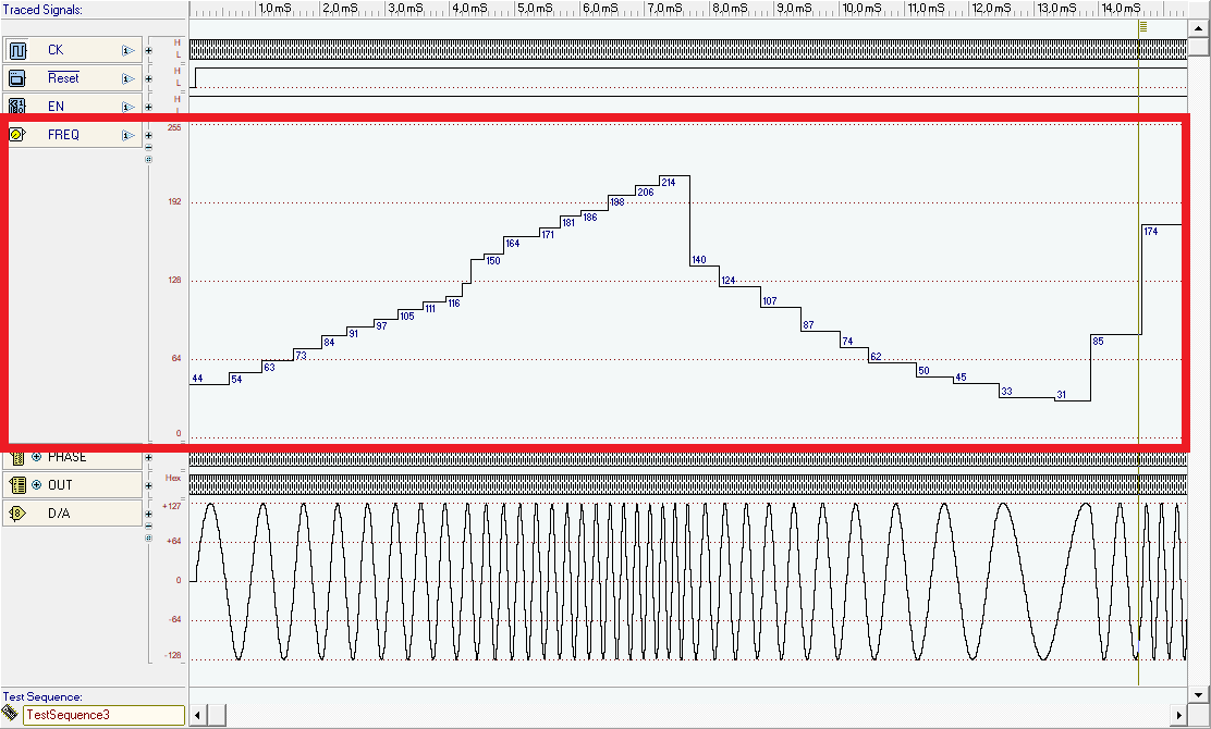
The numerical value, ranging from 0 to 255, and the transition time are defined manually with the mouse. This process is similar to defining other digital tracks.
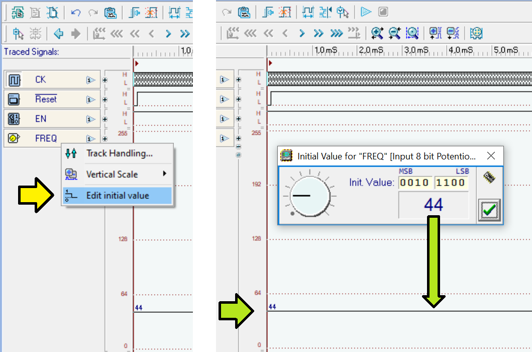
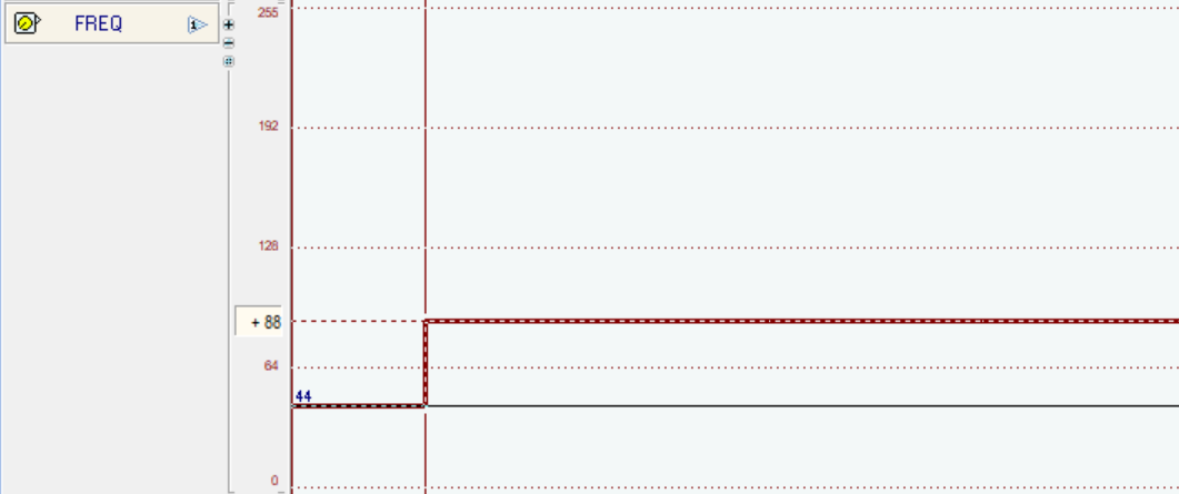
The following image displays the context menu item and the dialog box that is used to set the initial value. In this instance, the value is set to 44.
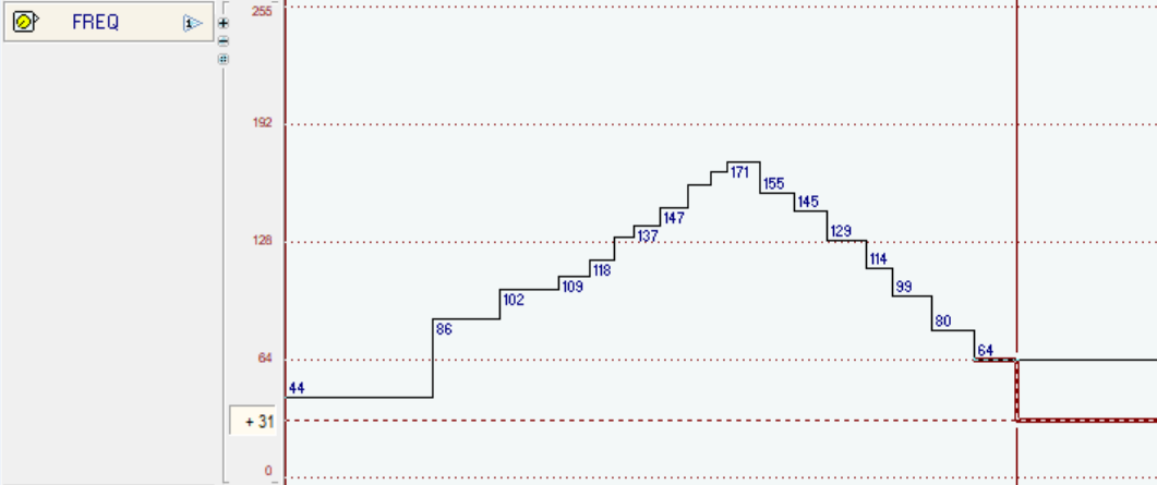
New values for t > 0 can be inserted by clicking on the potentiometer track and moving the new vertex along the time and amplitude axes. The new value is set with another click. The value being entered is displayed on the left.
You can input all the desired values step-by-step, but currently, you can only enter steps and not ramps.
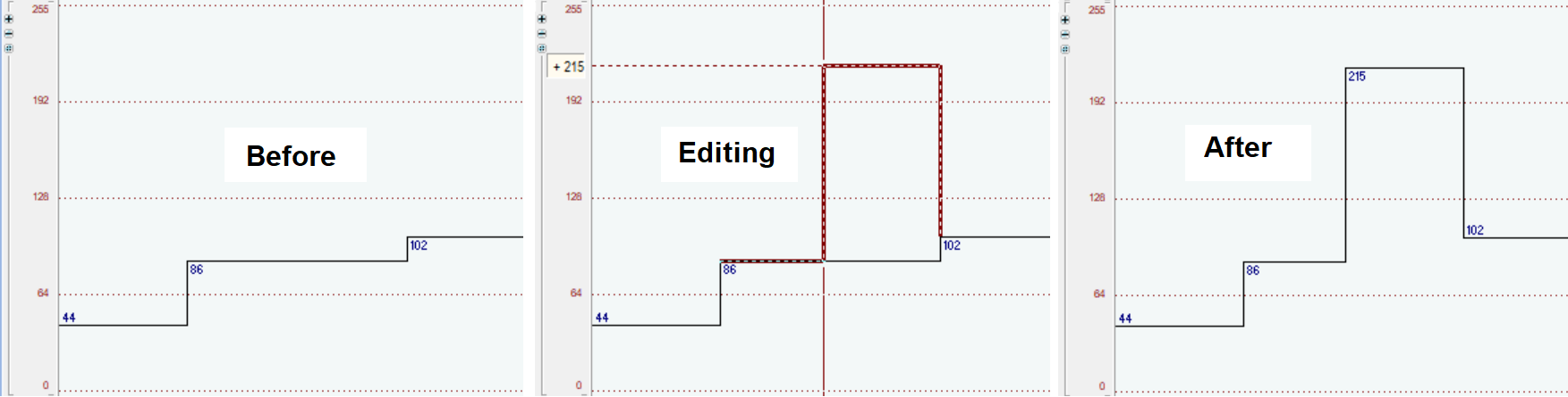
The values are displayed next to each variation, if the scale permits. You can also edit the curve by adding a new transition between two existing ones, as shown in the example below.
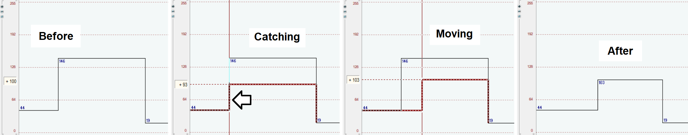
Additionally, you have the capability to adjust both edges and levels. Using the same command as previously demonstrated, click on an existing edge of the waveform and hold it with your mouse. By moving the mouse (without dragging), you can modify both the time and level of the existing transition. Another click will solidify these changes in the new position.
Edges can also be deleted. To activate the delete command, right-click on the desired track. Then, click between two edges of the waveform to delete the preceding transition, as shown in the following example.
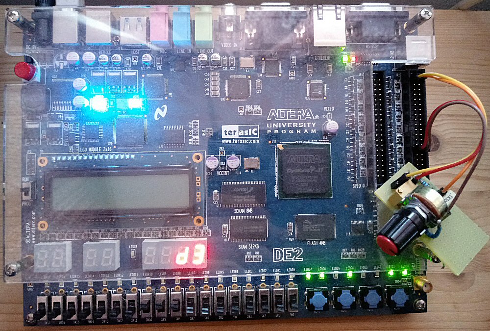
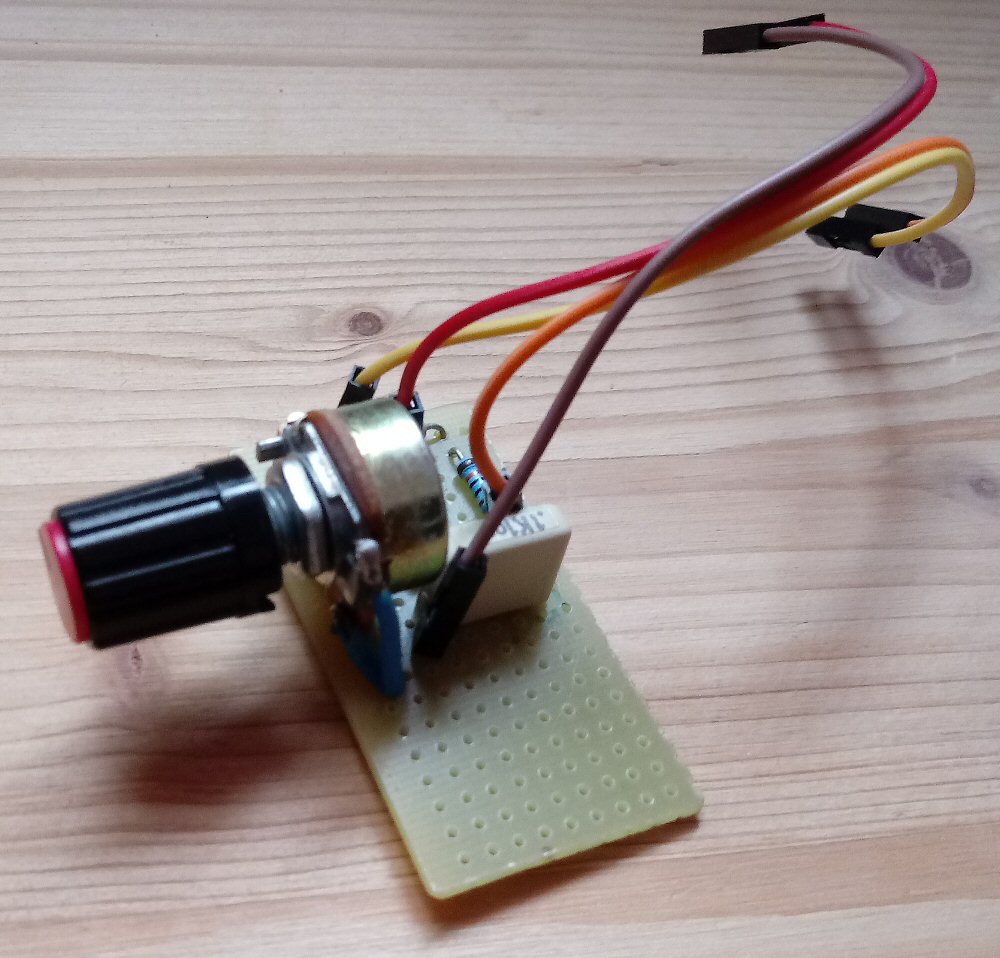
The potentiometer on FPGA
A small prototyping board can be used to connect a potentiometer to an FPGA board. The potentiometer is mounted on the board along with a capacitor and resistors. The four wires coming from the prototyping board enable the connection to the FPGA board.
FPGA cards, even the cheapest ones supported by Deeds, allow users to input parameters by turning a real knob. This method bypasses the need for an Analog-to-Digital Converter (ADC), which is typically required to convert the potentiometer's output voltage into a binary value. ADCs are not commonly found on most FPGA boards, particularly the more affordable options.
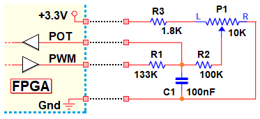
Deeds attempts to compensate for this deficiency by incorporating the ADC's functionality into the FPGA, at least as far as the necessary digital circuit is concerned. However, it remains necessary to utilize a small external analog circuit, the schematic of which is depicted in the following diagram.
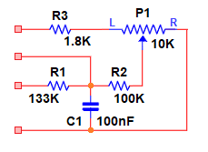
The Deeds implementation utilizes a PWM (Pulse Width Modulation) signal generator, which is modulated by a ramp of 256 distinct values. This PWM signal is transmitted out of a designated FPGA pin (labeled PWM in the accompanying diagram). Simultaneously, another FPGA pin (labeled POT) measures the algebraic sum of the PWM output and the voltage determined by the potentiometer's position. A capacitor is integrated into the circuit to filter out the high-frequency components of the PWM signal. The remaining two wires need to be connected to ground (GND) and the supply voltage (+3.3V), which are typically accessible on the headers of most FPGA boards.
The integrated digital network can identify the POT input's logical threshold crossing while the ramp is being generated, saving the corresponding number. This threshold will be crossed at different numbers as the potentiometer's position shifts. The resistor values are selected to allow the full range of 256 ramp levels to be read (with some margin at the extremes of the knob's rotation). The potentiometer is read approximately 8 times per second.
While this system is relatively slow and qualitative, it is still sufficient for reading a hand-controlled knob. Educational purposes don't necessarily require strict calibration, although adding trimmers to adjust resistors can precisely match the zero and maximum values to the potentiometer's limits.
Connecting the Potentiometer to the FPGA Pins
To test a prototype that includes a potentiometer on an Altera DE2 FPGA board, we'll use a simple network. The potentiometer will be connected to both a dual digit hex display and an 8-bit LED array. Click on the figure to open this example in the Deeds-DcS.

After opening the Test On FPGA window, you can connect the potentiometer to the FPGA board. To do this, choose the potentiometer from the circuit schematic on the left side of the window (see the following figure, arrow 1). A potentiometer connections panel will then appear on the right side.
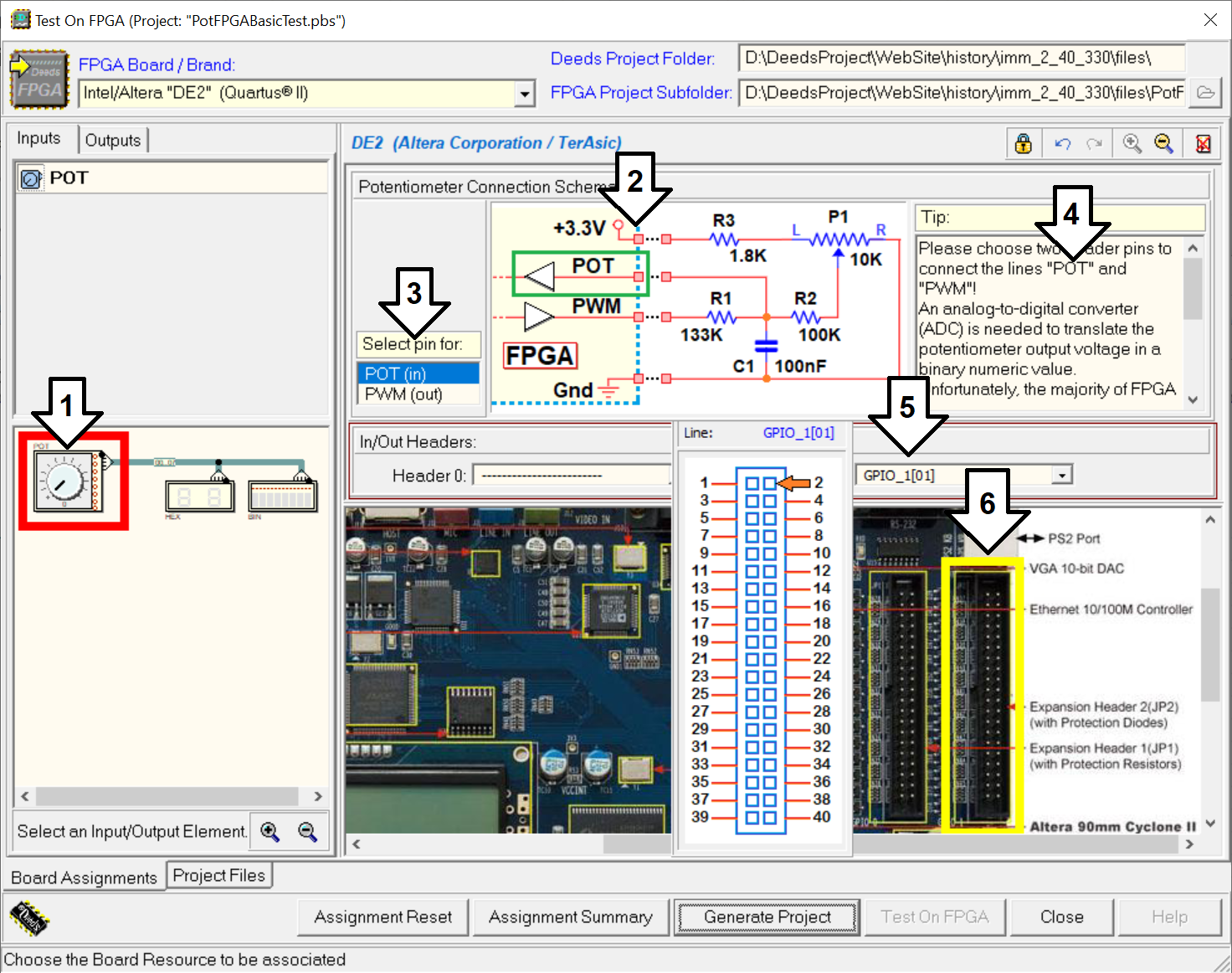
The FPGA pins must be connected to the potentiometer circuit depicted in the window (see arrow 2). The two POT or PWM connections needed can be chosen one at a time from the list box (highlighted by arrow 3). The instructions for completing these steps are briefly explained on the right side of the window (see arrow 4).
The POT line is connected to pin GPIO_1[01]' of Header 0, as shown in the figure (arrow 5). The location of this pin is highlighted in the connector's pin map (top view). Arrow 6 points to the connector on the FPGA board photo.
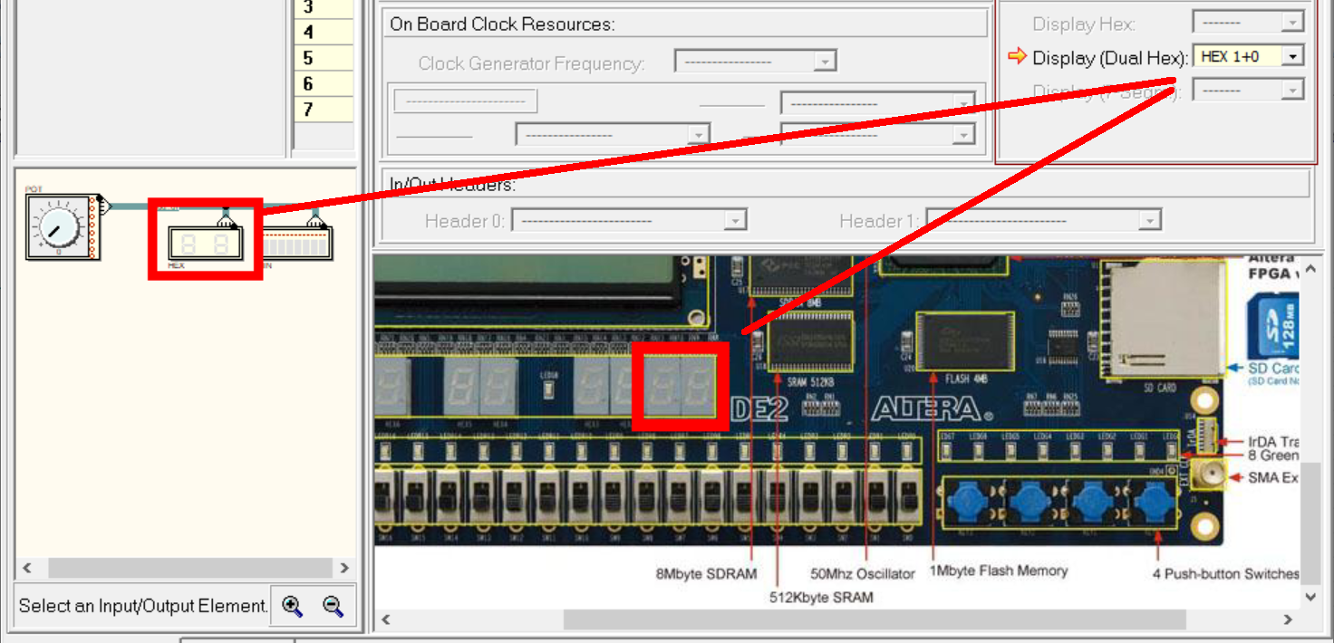
The process of assigning devices continues after designating the PWM line to the GPIO_1[00] pin on the same header. Next, we connect the dual hex display to two seven segment displays on the board, as illustrated in the following screenshot.
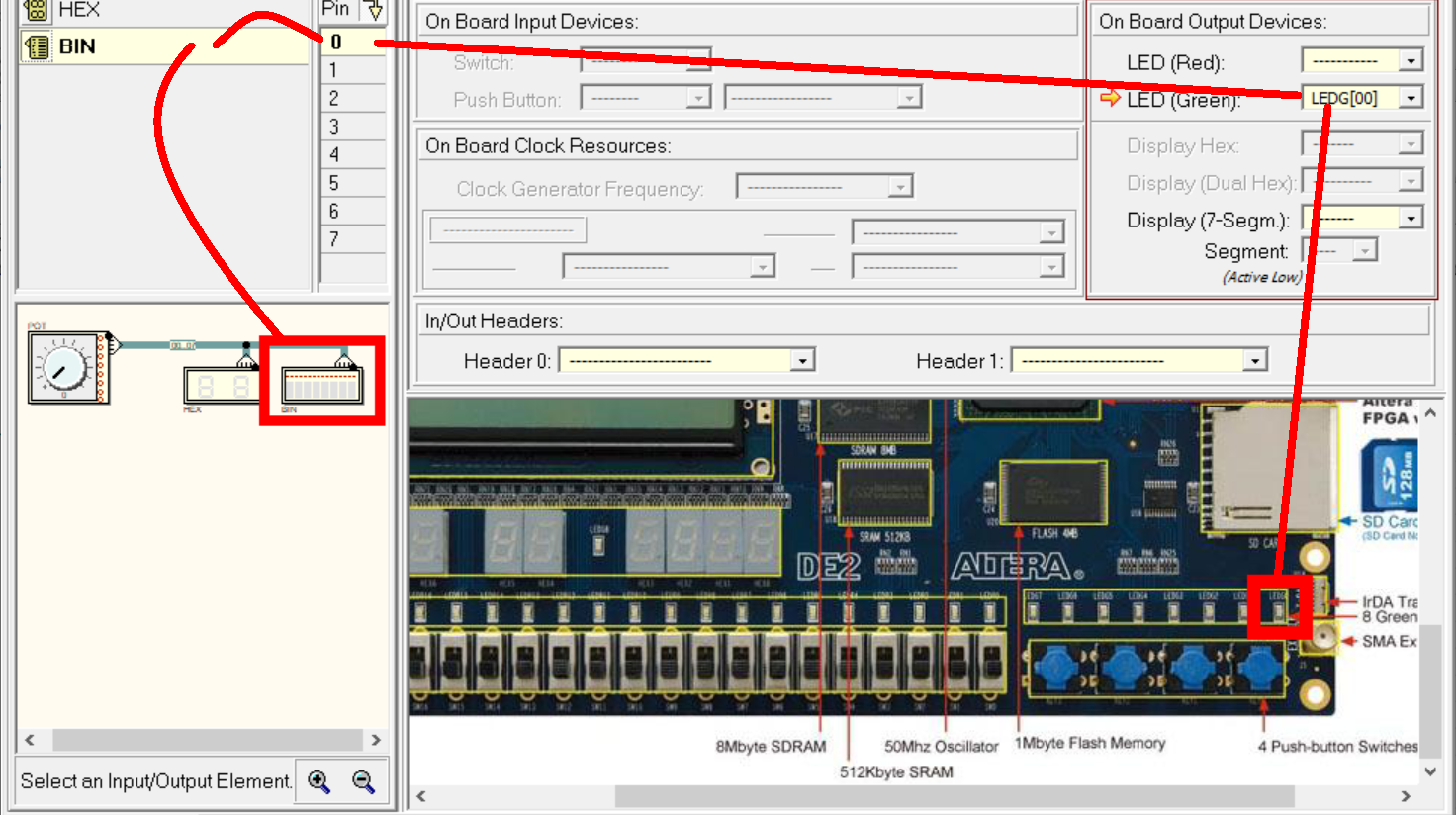
The screenshot below illustrates how the 8 LEDs of the arrow component are assigned to the 8 green LEDs on the board.
After the FPGA export process, we can see that the potentiometer circuit comprises two VHDL components. The PWM ramp generator (PotTimeBase) is instantiated only once in all projects. The second component, POT8, handles the POT signal reading and the 8-bit number capture and is instantiated to match the number of potentiometers in the circuit.

The image below shows a potentiometer connected to an Altera/Terasic DE2 board. The potentiometer has been adjusted to display the number D3h on the board's display, and the corresponding binary code '11010011' on the 8 green LEDs located at the bottom right of the board.